
D Flip-Flop with Synchronous Reset: Verilog Implementation
Advertisement
This article covers the design and implementation of a D flip-flop with a synchronous reset. We’ll explore the symbol, Verilog code, test bench, simulation results, and RTL schematic.
D Flip-Flop Symbol
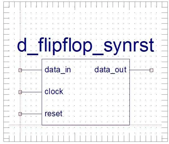
The following image depicts the symbol for a D flip-flop with a synchronous reset:
D Flip-Flop Verilog Code
Here’s the Verilog code for a D flip-flop with a synchronous reset:
module d_flipflop_synrst(data_in, data_out, clock, reset);
  input data_in;
  input clock, reset;
  output reg data_out;

  always @(posedge clock)
  begin
    if (reset)
      data_out <= 1'd0;
    else
      data_out <= data_in;
  end
endmodule


In this code:

- `data_in` is the input data.
- `clock` is the clock input. The flip-flop's state changes on the positive edge of the clock.
- `reset` is the synchronous reset input. When `reset` is high on a rising clock edge, the output `data_out` is set to 0.
- `data_out` is the output of the flip-flop.

## D Flip-Flop Verilog Code Testbench

This Verilog testbench verifies the functionality of the D flip-flop.

```verilog
module Tb_dflipflop_synrst();
  reg data_in;
  reg clock, reset;
  wire data_out;

  d_flipflop_synrst UUT(.data_in(data_in), .data_out(data_out), .clock(clock), .reset(reset));

  initial begin
    // Initialize Input Stimulus
    data_in = 0;
    clock = 0;
    reset = 0;
  end

  always #100 clock = ~clock;  // Generate a clock signal

  initial begin
    #200  data_in = 1'b1; reset = 1'b1;
    #200 data_in = 1'b1; reset = 1'b1;
    #300 data_in = 1'b1; reset=1'b0;
    #600 data_in = 1'b0;
    #500 data_in = 1'b1;
    #200 data_in = 1'b0;
    #400 $stop;
  end
endmodule
The testbench applies various input stimuli to the flip-flop and monitors the output to ensure correct behavior, including:
- Initializing inputs.
- Generating a clock signal with a period of 200 time units.
- Applying different values to
data_inandresetat different times. - Using
$stopto terminate the simulation.
D Flip-Flop Simulation
The simulation results should demonstrate the functionality of the D flip-flop, showing how the output changes based on the data input and clock signal, and how the reset input affects the output.

D Flip-Flop RTL Schematic
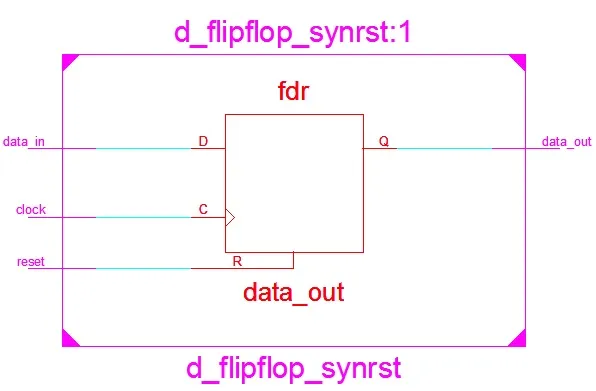
The RTL (Register-Transfer Level) schematic provides a graphical representation of the D flip-flop’s internal structure.
Explore Verilog Logic Gates, Mux & Encoders
- Verilog HDL Code for All Logic Gates
- 2-to-4 Decoder (Verilog HDL Code)
- 4-to-1 Multiplexer and 1-to-4 Demultiplexer (Verilog Code)
- Verilog Code: 1-to-4 Demultiplexer
- 8-to-1 Multiplexer (Verilog HDL Code)
- 8-to-3 Encoder Without Priority (Verilog)
- 8-to-3 Priority Encoder (Verilog)
- 8-to-3 Priority Encoder (Verilog Code)
- 1-Bit and 4-Bit Comparator Design (Verilog)
Explore Verilog Flip-Flops, Counters & Registers
- T, D, SR, JK Flip Flop (Verilog HDL Code)
- D Flip Flop Synchronous Reset (Verilog)
- D Flip Flop Without Reset (Verilog)
- Verilog Code for Binary Up-Down Counter
- Verilog HDL: BCD & Gray Counters
- 4-bit Down Counter (Verilog Code Test Bench)
- 4-bit Binary Asynchronous Reset Counter (Verilog)
- 4-bit Binary Synchronous Reset Counter (Verilog)
- 4-bit BCD Asynchronous Reset Counter (Verilog)
- 4-bit BCD Synchronous Reset Counter (Verilog Code)
- 4-bit Mod-13 Counter (Verilog Code Test Bench)
- Shift Left / Shift Right Register (Verilog)
- Parallel Load Shift Left Register (Verilog Code)
- PRBS Generator (Verilog Code Test Bench)
Explore Verilog Math, Processing & Memory
- Full Adder (Verilog HDL Code)
- Verilog Code: Half Adder, Half Subtractor, Full Subtractor
- 32-Bit ALU (Verilog Code)
- RAM / ROM (Verilog Code)
- Asynchronous FIFO (Verilog Code Test Bench)
- Asynchronous FIFO Design (Verilog Code and Explanation)
- Mealy / Moore Machine (Verilog)
- Low Pass FIR Filter (Verilog Code)
- 4-bit Binary to Gray Counter Converter in Verilog