
4-Bit Binary Synchronous Reset Counter in Verilog
By RF Wireless Expert Team
Advertisement
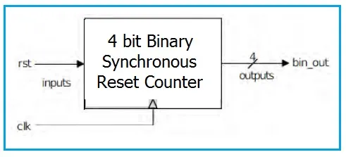
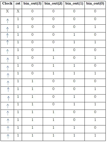
This page provides the Verilog source code for a 4-bit binary synchronous reset counter. You’ll also find the block diagram and truth table to help understand how it works.
Block Diagram
Here’s a block diagram of the 4-bit binary synchronous reset counter:
Truth Table
The following truth table illustrates the counter’s behavior:
4 Bit Binary Synchronous Reset Counter Verilog Code
module bin_sync(
    clk,
    rst,
    bin_out
);

input clk, rst;
output [3:0] bin_out;

reg [3:0] bin_out;
reg [22:0] div; // Added a clock divider
reg clkdiv;      // Clock divider output

initial bin_out = 4'b0000;
initial div = 23'b0;       // Initialize the divider

always @ (posedge clk) begin
    div <= div + 1'b1; // Increment the divider at each clock edge
    clkdiv <= div[22]; // Use the MSB as a divided clock
end

always @ (posedge clkdiv) begin
    if (rst == 1)
        bin_out <= 4'b0000;  // Reset to zero when rst is high
    else
        bin_out <= bin_out + 4'b0001; // Increment on clock edge when not reset
end

endmodule
Explanation:
- Module Declaration: The
bin_syncmodule hasclk(clock),rst(reset), andbin_out(4-bit output) as input and output signals, respectively. - Internal Register:
bin_outis declared as a 4-bit register to hold the counter’s value. A 23-bit registerdivand a 1-bit registerclkdivare added to divide the input clock. - Initialization: The
initialblock sets the initial value ofbin_outto 0000. - Clock Division: The
always @(posedge clk)block implements a simple clock divider. Thedivregister increments on every rising edge of the input clock. The 22nd bit (MSB) of thedivregister is assigned toclkdiv, effectively dividing the input clock frequency by 222 = 4194304. - Counter Logic: The
always @(posedge clkdiv)block describes the counter’s behavior. When the reset signalrstis high,bin_outis reset to 0000. Otherwise, on each rising edge of the divided clockclkdiv,bin_outis incremented by 1.
Explore Verilog Logic Gates, Mux & Encoders
- Verilog HDL Code for All Logic Gates
- 2-to-4 Decoder (Verilog HDL Code)
- 4-to-1 Multiplexer and 1-to-4 Demultiplexer (Verilog Code)
- Verilog Code: 1-to-4 Demultiplexer
- 8-to-1 Multiplexer (Verilog HDL Code)
- 8-to-3 Encoder Without Priority (Verilog)
- 8-to-3 Priority Encoder (Verilog)
- 8-to-3 Priority Encoder (Verilog Code)
- 1-Bit and 4-Bit Comparator Design (Verilog)
Explore Verilog Flip-Flops, Counters & Registers
- T, D, SR, JK Flip Flop (Verilog HDL Code)
- D Flip Flop Synchronous Reset (Verilog)
- D Flip Flop Without Reset (Verilog)
- Verilog Code for Binary Up-Down Counter
- Verilog HDL: BCD & Gray Counters
- 4-bit Down Counter (Verilog Code Test Bench)
- 4-bit Binary Asynchronous Reset Counter (Verilog)
- 4-bit Binary Synchronous Reset Counter (Verilog)
- 4-bit BCD Asynchronous Reset Counter (Verilog)
- 4-bit BCD Synchronous Reset Counter (Verilog Code)
- 4-bit Mod-13 Counter (Verilog Code Test Bench)
- Shift Left / Shift Right Register (Verilog)
- Parallel Load Shift Left Register (Verilog Code)
- PRBS Generator (Verilog Code Test Bench)
Explore Verilog Math, Processing & Memory
- Full Adder (Verilog HDL Code)
- Verilog Code: Half Adder, Half Subtractor, Full Subtractor
- 32-Bit ALU (Verilog Code)
- RAM / ROM (Verilog Code)
- Asynchronous FIFO (Verilog Code Test Bench)
- Asynchronous FIFO Design (Verilog Code and Explanation)
- Mealy / Moore Machine (Verilog)
- Low Pass FIR Filter (Verilog Code)
- 4-bit Binary to Gray Counter Converter in Verilog