
MAX2871 Wideband PLL VCO IC Pin Diagram, Circuit and Applications
Advertisement
The MAX2871 is an integrated fractional/integer-N PLL with a built-in wideband VCO capable of generating stable RF signals over a broad frequency range. It is commonly used in wireless communication equipment, radar systems, RF test instruments, and microwave transceivers. This article covers the MAX2871 pin diagram, working, circuit design, features, and applications.
Key features of MAX2871
- Ultra-Wide Frequency Range: Synthesizes frequencies from 23.5MHz up to 6000MHz (6 GHz) using multiple integrated VCOs and output binary dividers (divide ratios of 1/2/4/8/16/32/64/128).
- Excellent Noise Performance: Features a low normalized in-band phase noise of -230 dBc/Hz, reducing the system’s noise floor contribution.
- Dual Programmable Outputs: Features dual differential output drivers that can be independently programmed to deliver -1dBm to +8dBm differential output power (or -4dBm to +5dBm single-ended). Both outputs can be muted via software or hardware.
- Phase Synchronization & Adjustment: Allows the output phase to be reset and adjusted, enabling the precise synchronization of multiple MAX2871 synthesizers to a single reference input.
- Fast Switching & Lock Times: Includes manual and automatic VCO selection, cycle slip reduction, and fast-lock features to improve frequency acquisition time.
- Integrated Temperature Sensor: Includes an on chip temperature sensor with a 7-bit ADC to ensure optimum VCO selection and glitch free operation over the entire temperature range (-40°C to +85°C).
- Flexible Interface: Controlled via a 4-wire serial interface (SPI) compatible with 1.8V control logic.
MAX2871 Pin Diagram
Here’s a look at the MAX2871 pin diagram:
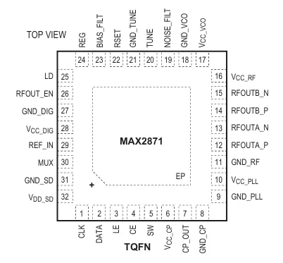
| Pin | Name | Function |
|---|---|---|
| 1 | CLK | Serial clock input for the SPI-compatible interface. Data is latched on the rising edge. |
| 2 | DATA | Serial data input (MSB first). Used to program the internal registers. |
| 3 | LE | Load Enable. Transfers the shifted data into the selected register. |
| 4 | CE | Chip Enable. Logic Low powers down the synthesizer; Logic High enables normal operation. |
| 5 | SW | Fast-lock switch connection for the loop filter. Leave unconnected if fast-lock mode is not used. |
| 6 | VCC_CP | Charge Pump Power Supply. VP must have the same value as AVDD. |
| 7 | CP_OUT | Charge pump output connected to the external PLL loop filter. |
| 8 | GND_CP | Ground for the charge pump section. |
| 9 | GND_PLL | Ground for the PLL circuitry. |
| 10 | VCC_PLL | PLL power supply input. |
| 11 | GND_RF | Ground for the RF output stage. |
| 12 | RFOUTA_P | Positive differential RF Output A. |
| 13 | RFOUTA_N | Negative differential RF Output A. |
| 14 | RFOUTB_P | Positive differential RF Output B. |
| 15 | RFOUTB_N | Negative differential RF Output B. |
| 16 | VCC_RF | External precision resistor connection used to set internal bias current. |
| 17 | VCC_VCO | Additional VCO supply pin. Connect to the same supply as Pin 14. |
| 18 | GND_VCO | Additional VCO ground connection. |
| 19 | NOISE_FILT | Loop filter node used to reduce VCO noise. Connect an external bypass capacitor. |
| 20 | TUNE | VCO tuning voltage input from the external PLL loop filter. |
| 21 | GND_TUNE | Ground reference for the tuning circuitry. |
| 22 | RSET | Charge-Pump Current Range Input. Connect an external resistor to ground to set the minimum CP current. |
| 23 | BIAS_FILT | I VCO Noise Decoupling. Place a 1µF capacitor to ground. |
| 24 | REG | Reference Voltage Compensation. Place a 1µF capacitor to ground. |
| 25 | LD | Lock Detect Output. |
| 26 | RFOUT_EN | RF Output Enable. A logic-low disables the RF outputs. A. |
| 27 | GND_DIG | Ground for Digital Circuitry. Connect to main board ground plane, not directly to the paddle. A. |
| 28 | VCC_DIG | Power Supply for Digital Circuitry. Place decoupling capacitors as close as possible to pin. |
| 29 | REF_IN | Reference Frequency Input. |
| 30 | MUX | Multiplexed I/Os. |
| 31 | GND_SD | Ground for Sigma-Delta Modulator. |
| 32 | VDD_SD | Power Supply for Sigma-Delta Modulator. |
Example Use Case : MAX2871 as Wideband RF Signal Generator for Test Equipment
The Scenario: A manufacturer is building a piece of laboratory test equipment (like a spectrum analyzer or a programmable signal generator) that needs to test various RF components operating at different frequency bands (e.g., VHF, UHF, Wi-Fi and sub-6GHz 5G).
How the MAX2871 is used: Instead of using multiple discrete oscillators for different frequency bands, the designer can use a single MAX2871. By leveraging its internal binary dividers and multiple VCO cores, the system can sweep through a massive frequency range of 23.5 MHz all the way up to 6 GHz. The dual outputs allow the signal to be routed to different test ports, and the programmable output power allows the equipment to dynamically adjust the signal strength injected into the Device Under Test (DUT).
Applications of MAX2871
- Wireless Infrastructure
- Test and Measurement
- Clock Generation
- Microwave Radios
Summary
The MAX2871 integrates a PLL and wideband VCO into a single IC for flexible RF frequency synthesis. It is widely used in microwave and wireless communication systems.
Continue Learning Voltage Controlled Oscillators (VCO)
Deep dives into how voltage controlled oscillators generate frequencies, how they are tuned, and how they integrate with PLLs.
- Voltage Controlled Oscillators (VCOs) Overview
- VCO Basics (Voltage Controlled Oscillators)
- VCO Tuning Constant and Tuning Methods
- Difference Between VCO and PLL
- NCO vs VCO: Understanding the Differences
- VCO vs VCXO Differences
- MAX2871 Wideband PLL/VCO IC: Pin Diagram and Applications
Explore Phase-Locked Loops (PLL) & IC Applications
Understand the core mechanics of Phase Locked Loops and explore application notes for popular PLL chips used in RF design.