
AD8318 RF Power Detector IC Pin Diagram, Circuit and Applications
Advertisement
The AD8318 is a high performance RF logarithmic power detector IC that measures RF signal strength over a broad frequency range with excellent accuracy. It is commonly used in wireless infrastructure, RF instrumentation, transmit power monitoring, and automatic gain control systems. This article discusses its pin diagram, working principle, circuit, features, and applications.
Key features of AD8318
- Wide Bandwidth: Operates from 1 MHz up to 8 GHz.
- High Accuracy: +/- 1.0 dB over a 55 dB range (for frequencies < 5.8 GHz).
- High Temperature Stability: Logarithmic intercept stability of +/- 0.5 dB over temperature variations.
- Fast Response Time: 10 ns fall time and 12 ns rise time, enabling RF burst detection at repetition rates beyond 45 MHz.
- Integrated Temperature Sensor: Provides a 2 mV/ degreeC slope output for additional system monitoring.
- Low Power/Power Down: Operates on a single 5 V supply at 68 mA. A power down (sleep) feature reduces power consumption to <1.5 mW when disabled.
- Compact Packaging: Available in a small footprint 4 mm × 4 mm, 16-lead LFCSP. Low Noise Output: Minimal wideband noise on the measurement/controller output (VOUT).
AD8318 Pin Diagram
Here’s a look at the AD8307 pin diagram:
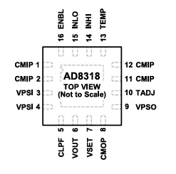
| Pin No. | Pin Name | Type | Function |
|---|---|---|---|
| 1 | CMIP | Ground | Input system ground. Connect to PCB ground. |
| 2 | CMIP | Ground | Input system ground. |
| 3 | VPSI | Power | Positive supply voltage for the input section (4.5 V to 5.5 V). |
| 4 | VPSI | Power | Positive supply voltage. Tie to Pin 3. |
| 5 | CLPF | Analog | Loop filter capacitor connection. An external capacitor connected here determines response time and output filtering. |
| 6 | VOUT | Output | Logarithmic detector output. Provides a DC voltage proportional to the RF input power. Also serves as the controller output in closed-loop applications. |
| 7 | VSET | Input | Setpoint input for controller mode. In measurement mode, connect to VOUT to establish detector operation. |
| 8 | CMOP | Ground | Output system ground. Connect to PCB ground. |
| 9 | VPSO | Power | Positive supply voltage for the output section (4.5 V to 5.5 V). Connect to the same supply as VPSI. |
| 10 | TADJ | Analog | Temperature compensation adjustment input. Used with an external resistor for improved temperature stability. |
| 11 | CMIP | Ground | Input system ground. |
| 12 | CMIP | Ground | Input system ground. |
| 13 | TEMP | Output | Temperature sensor output with approximately 2 mV/°C slope for monitoring device temperature. |
| 14 | INHI | RF Input | RF signal input. Accepts RF signals from approximately −60 dBm to 0 dBm (50 Ω system). AC-coupled. |
| 15 | INLO | RF Input | RF return (RF common) for the differential RF input. AC-coupled. |
| 16 | ENBL | Digital Input | Enable control. Connect to VPSI for normal operation or to ground to place the IC in low-power shutdown mode. |
Example Use Case : AD8318 as Automatic Gain Control Loop
A prominent use case detailed in the datasheet is using the AD8318 in Controller Mode to provide Automatic Gain Control (AGC) in combination with a Variable Gain Amplifier (VGA), such as the AD8367 or ADL5330.
How it works:
Setup: The link between the VSET and VOUT pins is broken (which would normally be connected for simple measurement mode).
Setpoint Applied: A specific “setpoint” DC voltage is applied to the VSET pin. This represents the desired target RF power level.
Feedback Loop: The AD8318’s output (VOUT) is connected directly to the gain control terminal of the VGA. The output of the VGA is then fed back into the RF input of the AD8318 (often using a directional coupler).
Operation: An incoming RF signal with a varying, unpredictable amplitude enters the VGA. The AD8318 measures the VGA’s output and compares it to the VSET voltage. It then acts as an error amplifier, dynamically raising or lowering the voltage on VOUT to adjust the VGA’s gain.
Result: The loop stabilizes when the RF level hitting the AD8318 matches the applied VSET voltage. This ensures the output of the VGA remains at a constant, optimized amplitude (over approx. 45 dB dynamic range), yielding the highest possible signal to noise ratio (SNR) for downstream components like Analog to Digital Converters (ADCs).
Applications of AD8318
- RF transmitter Power Amplifier (PA) setpoint control and level monitoring.
- Received Signal Strength Indicator (RSSI) measurement in base stations, WLAN, WiMAX, and radar systems.
Summary
The AD8318 enables accurate RF power measurement over a wide dynamic range. Its compact design makes it suitable for modern wireless and instrumentation applications.