
AD8307 Log Detector IC Pin Diagram, Circuit and Applications
Advertisement
The AD8307 is a precision logarithmic detector IC from Analog Devices designed for accurate RF and IF signal level measurement over a wide dynamic range. It converts input signal amplitude into a logarithmic voltage output, making it suitable for power measurement, RSSI systems, automatic gain control (AGC), spectrum monitoring, and wireless communication equipment. This article explains the AD8307 pin diagram, internal working, circuit implementation, key features, and practical applications.
Key features of AD8307
- High Dynamic Range: Offers a 92 dB dynamic range (from –75 dBm to +17 dBm, and down to -90 dBm using an input matching network).
- Wide Frequency Range: Operates from DC up to 500 MHz with +/- 1 dB linearity.
- Precise Scaling: Provides a nominal logarithmic slope of 25 mV/dB and an intercept of -84 dBm, which are highly stable over temperature variations.
- Low Power Consumption: Operates on a single supply voltage of 2.7 V to 5.5 V, drawing a typical current of just 7.5 mA.
- Fast Response & Standby: Features a 100 ns power-up time and a CMOS compatible enable pin that drops sleep current to 150 μA.
- Fully Differential: Utilizes a fully differential DC coupled signal path for high stability and common mode noise rejection.
AD8307 Pin Diagram
Here’s a look at the AD8307 pin diagram:
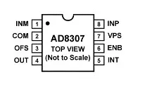
| Pin No. | Pin Name | Type | Function |
|---|---|---|---|
| 1 | INM | Input | Negative RF signal input. Normally biased internally near half the supply voltage. Together with INP forms the differential RF input. |
| 2 | COM | Ground | Common reference pin. Normally connected to system ground. |
| 3 | OFS | Analog | Offset adjustment pin. Used with an external capacitor to improve output stability and reduce noise. |
| 4 | OUT | Output | Logarithmic (RSSI) output voltage. Provides a DC voltage proportional to the logarithm of the input signal amplitude. |
| 5 | INT | Analog | Intercept adjustment pin. Used to fine-tune the logarithmic intercept (approximately ±3 dB adjustment). |
| 6 | ENB | Digital Input | Chip enable/disable control. Logic High enables normal operation, while Logic Low places the device in low-power standby mode. |
| 7 | VPS | Power | Positive power supply input. Operating supply range is 2.7 V to 5.5 V. |
| 8 | INP | Input | Positive RF signal input. Used together with INM as the differential RF input. The polarity of INP and INM is not critical because of the detector’s symmetrical input structure. |
Example Use Case : AD8307 based Power Meter
The Scenario: A system needs to measure the massive power output being delivered from a transmitter’s final amplifier to an antenna, spanning from 1 μW (–30 dBm) all the way up to 1 kW (+ 60 dBm).
How AD8307 is used: Because the AD8307 natively measures up to + 17 dBm, it cannot handle a 1 kW signal directly. However, by placing a shielded, capacitive or resistive voltage divider at the front end input, the signal is attenuated by a nominal ratio of 158:1 (44 dB).
The Result: This attenuation shifts the AD8307’s intercept from −84 dBm to −40 dBm. The AD8307 will now output a safe, scaled DC voltage directly corresponding to the massive power levels (e.g. reading 1.5 V for 100 mW, 2.0 V for 10 W, and 2.5 V for 1 kW).
Applications of AD8307
- Conversion of radio frequency (RF) signal levels to decibel form.
- Transmitter antenna power measurement.
- Receiver signal strength indication (RSSI).
- Low cost radar and sonar signal processing.
- Network and spectrum analyzers (can be extended to 120 dB dynamic range).
- Signal level determination down to very low frequencies (20 Hz).
- True decibel AC mode for multimeters.
Summary
The AD8307 offers accurate logarithmic signal detection across a wide frequency range. Its high dynamic range and simple interface make it an excellent choice for RF measurement and instrumentation systems.