
ADF4351 Fractional N PLL Synthesizer IC Pin Diagram, Circuit and Applications
Advertisement
The ADF4351 is a widely used fractional-N frequency synthesizer integrating a PLL and VCO to generate precise RF output frequencies. It is suitable for signal generators, SDR platforms, wireless communication equipment, instrumentation, and microwave applications. This article explains the ADF4351 pin diagram, working, circuit implementation, specifications, and applications.
Key features of ADF4351
- Wide Output Frequency Range: 35 MHz to 4400 MHz, achieved via an integrated voltage controlled oscillator (VCO) with a fundamental range of 2200 MHz to 4400 MHz and programmable output dividers (divide-by-1/-2/-4/-8/-16/-32/-64).
- Dual Synthesizer Modes: Operates as both a fractional-N and integer-N phase-locked loop (PLL) synthesizer.
- Low Phase Noise & High Precision: Features a low phase noise VCO, typical rms jitter of 0.3 ps, and a typical Error Vector Magnitude (EVM) of 0.4% at 2.1 GHz.
- Programmable Output: Programmable output power levels (–4 dBm to +5 dBm in 3 dB steps) and an RF output mute function (both pin- and software-controllable) for applications requiring isolation.
- Auxiliary Output: Includes a secondary (auxiliary) RF output stage that can be used to drive another circuit or powered down when not in use.
- Fast Lock & Cycle Slip Reduction: Includes a switched bandwidth fast lock mode and cycle slip reduction to dramatically improve lock times without modifying loop filter circuitry.
- Control Interface: Simple 3-wire serial interface (SPI compatible).
- Power Supply & Logic: Operates on a 3.0 V to 3.6 V power supply with 1.8 V logic compatibility and features software/hardware power-down modes.
ADF4351 Pin Diagram
Here’s a look at the ADF4351 pin diagram:
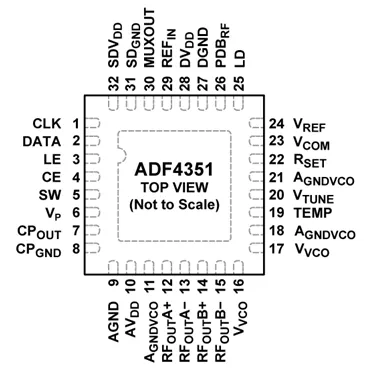
| Pin | Name | Function |
|---|---|---|
| 1 | CLK | Serial clock input for the 3-wire SPI-compatible interface. |
| 2 | DATA | Serial data input (MSB first) used to program internal registers. |
| 3 | LE | Load Enable. Transfers serial data from the shift register into the selected register. |
| 4 | CE | Chip Enable. High enables normal operation; Low powers down the device. |
| 5 | SW | Fast-lock switch output used with the external loop filter. |
| 6 | VP | Charge pump supply voltage. |
| 7 | CP OUT | Charge pump output connected to the external PLL loop filter. |
| 8 | CPGND | Ground for the charge pump circuitry. |
| 9 | AGND | Analog ground connection. |
| 10 | AVDD | Analog power supply (3.0 V to 3.6 V). |
| 11 | AGNDVCO | Ground for the VCO |
| 12 | RFOUTA+ | Primary VCO output. |
| 13 | RFOUTA- | Complementary VCO output. |
| 14 | RFOUTB+ | Auxiliary VCO output. |
| 15 | RFOUTB- | Complementary Auxiliary VCO output. |
| 16 | VVCO | VCO supply voltage. |
| 17 | VVCO | Additional VCO supply pin. Connect to the same supply as Pin 16. |
| 18 | AGNDVCO | Ground for the VCO |
| 19 | TEMP | Internal temperature sensor/output used during factory calibration. Normally bypassed with a capacitor. |
| 20 | VTUNE | Control Input to the VCO. |
| 21 | AGNDVCO | Ground for the VCO |
| 22 | RSET | Connect a precision resistor (typically 5.1 kΩ) to ground to set the charge pump current. |
| 23 | VCOM | Internal compensation node. Bypass with an external capacitor placed close to the pin. |
| 24 | VREF | Reference voltage decoupling pin. Connect a bypass capacitor to ground. |
| 25 | LD | Lock Detect output. High indicates PLL lock; Low indicates unlocked condition. |
| 26 | PDBRF | RF output power-down control. Low mutes the RF outputs. Can also be software controlled. |
| 27 | DGND | Digital Ground |
| 28 | DVDD | Digital logic supply voltage. Must be equal to AVDD. |
| 29 | REFIN | Reference clock input. Accepts CMOS, TTL, or AC-coupled sinusoidal reference signals. |
| 30 | MUXOUT | Multiplexed output configurable for lock detect, R-counter, N-divider, analog lock detect, and diagnostic signals. |
| 31 | SDGND | Digital Σ-Δ Modulator Ground. Ground return pin for the Σ-Δ modulator. |
| 32 | SDVDD | Supply voltage for the digital Σ-Δ modulator. Must be equal to AVDD. |
Example Use Case : ADF4351 as Direct Conversion Modulator for Base Station Transmitters
A prominent system-level use case for the ADF4351 is acting as the Local Oscillator (LO) in a direct conversion transmitter architecture, heavily used in modern base stations. The ADF4351 is paired with a dual integrated digital to analog converter (like the AD9788 TxDAC) and an I/Q modulator (like the ADL5375).
The ADF4351 generates the LO frequency. Its complementary differential outputs directly drive the differential LO input ports of the ADL5375 modulator.
Applications of ADF4351
- Wireless Infrastructure: Base station applications including W-CDMA, TD-SCDMA, WiMAX, GSM, PCS, DCS, and DECT.
- Test Equipment
- Wireless LANs (WLANs)
- CATV Equipment
- Clock Generation
Summary
The ADF4351 provides flexible RF frequency synthesis with excellent phase noise performance. It is one of the most popular PLL synthesizer ICs for RF development.
Continue Learning Frequency Synthesizers
Resources on synthesizing complex frequencies for RF transmission, covering design, settling time, and Direct Digital Synthesis (DDS).