
ADF4002 PLL IC Pin Diagram, Circuit and Applications
Advertisement
The ADF4002 is a high-performance phase-locked loop IC designed for integer-N frequency synthesis applications requiring low phase noise and excellent frequency stability. It is widely used in wireless communication equipment, instrumentation, local oscillators, and RF transceivers. This article explains its pin diagram, working principle, circuit, features, and applications.
Key features of ADF4002 PLL
- Bandwidth: 400 MHz
- Power Supply: 2.7 V to 3.3 V
- Extended Tuning Voltage: A separate charge pump supply (Vp) allows for an extended tuning voltage in 3 V systems (up to 5.5 V).
- Programmability: Features programmable charge pump currents and a 14 bit reference counter (R counter) and 13-bit N counter.
- Interface: 3-wire serial interface (SPI compatible) supporting up to 20 MHz clock rates.
- Lock Detect: Supports both analog and digital lock detect.
- Power Management: Includes both hardware and software power down modes.
- Phase Detector: 104 MHz phase detector frequency with a very low normalized phase noise floor (–222 dBc/Hz).
ADF4002 PLL Pin Diagram
Here’s a look at the ADF4002 PLL pin diagram:
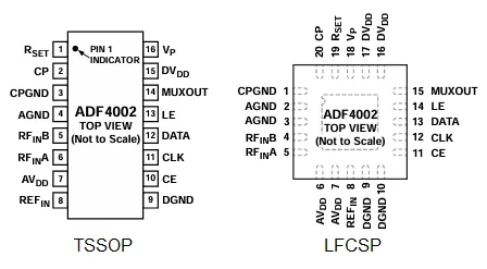
| Pin No. | Pin Name | Type | Function |
|---|---|---|---|
| 1 | RSET | Analog | Connect an external precision resistor (typically 5.1 kΩ) to CPGND to set the maximum charge pump output current. |
| 2 | CP | Analog Output | Charge pump output. Connects to the external PLL loop filter, which drives the VCO tuning voltage. |
| 3 | CPGND | Ground | Ground return for the charge pump circuitry. |
| 4 | AGND | Ground | Analog ground for the RF input and analog circuitry. |
| 5 | RFINB | RF Input | Complementary RF input to the phase-frequency detector. Normally AC-coupled and paired with RFINA for differential operation. |
| 6 | RFINA | RF Input | Primary RF input from the external VCO or divider. Accepts the feedback signal for PLL operation. |
| 7 | AVDD | Power | Analog supply voltage (2.7 V to 3.3 V). Decouple close to the pin. |
| 8 | REFIN | Input | Reference clock input. Accepts CMOS, TTL, or AC-coupled sine-wave reference signals. |
| 9 | DGND | Ground | Digital ground reference. |
| 10 | CE | Digital Input | Chip Enable. Logic Low powers down the synthesizer and places the charge pump in high-impedance mode. Logic High enables normal operation. |
| 11 | CLK | Digital Input | Serial clock input for the 3-wire SPI-compatible programming interface. |
| 12 | DATA | Digital Input | Serial data input (MSB first) used to program the internal registers. |
| 13 | LE | Digital Input | Load Enable. Transfers the serial data from the shift register into the selected control register. |
| 14 | MUXOUT | Digital Output | Multiplexed output. Can be programmed to provide digital lock detect, analog lock detect, R-counter output, N-counter output, or other diagnostic signals. |
| 15 | DVDD | Power | Digital supply voltage (2.7 V to 3.3 V). Should be the same voltage as AVDD. |
| 16 | VP | Power | Charge pump supply voltage. Can be higher than DVDD (up to 5.5 V) to support VCOs requiring a wider tuning voltage range. |
Example Use Case : ADF4002 as Standalone Phase Frequency Detector (PFD)
Because the ADF4002 allows both the R and N counters to be programmed to exactly 1, the device can effectively bypass the division and act as a standalone PFD and charge pump.
Setup: The reference frequency is fed directly into the PFD (R=1). The charge pump output integrates into a control voltage for a VCXO, which is then divided down to the desired frequency using an external prescaler/divider.
Result: This is particularly useful in “clock cleaning” applications or for creating a high performance LO, taking advantage of the device’s extremely low in-band phase noise floor.
Applications of ADF4002
- Clock conditioning
- Clock generation
- IF LO (Intermediate Frequency Local Oscillator) generation
- Upconversion and downconversion sections of wireless receivers and transmitters.
Summary
The ADF4002 offers reliable frequency synthesis with low phase noise and high stability. It is suitable for RF communication and instrumentation systems.
Continue Learning Frequency Synthesizers
Resources on synthesizing complex frequencies for RF transmission, covering design, settling time, and Direct Digital Synthesis (DDS).