
LMX2594 Microwave PLL IC Pin Diagram, Circuit and Applications
Advertisement
The LMX2594 is a high-performance microwave PLL frequency synthesizer capable of generating low-noise RF and microwave signals up to multi-gigahertz frequencies. It is widely used in radar systems, 5G infrastructure, test equipment, satellite communication, aerospace, and microwave instrumentation. This article covers the LMX2594 pin diagram, working principle, circuit design, features, and practical applications.
Key features of LMX2594
- Wide Output Frequency Range: 10 MHz to 15 GHz.
- Ultra-Low Noise & Jitter:
- Phase noise of –110 dBc/Hz at a 100-kHz offset (with a 15 GHz carrier).
- 45-fs rms jitter at 7.5 GHz (100 Hz to 100 MHz).
- PLL Figure of Merit (FOM) of –236 dBc/Hz and normalized 1/f noise of –129 dBc/Hz.
- Advanced Phase Detector: Operates at up to 400 MHz in integer mode and 300 MHz in fractional mode, featuring a 32-bit fractional-N divider.
- Spur Mitigation: Features a programmable input multiplier to remove integer boundary spurs.
- Multi-Device Phase Synchronization: Allows the output phase to be synchronized across multiple devices for deterministic phase relationships.
- SYSREF / JESD204B Support: Capable of generating or repeating SYSREF signals with a fine 9-ps resolution programmable delay to account for board trace differences.
- Ramping & Chirp Generation: Built-in frequency ramping (automatic or manual) and chirp generation capabilities, ideal for FMCW applications.
- Fast Calibration: VCO calibration speed of < 20 µs.
- Simplified Power Design: Operates from a single 3.3 V supply with integrated LDOs, eliminating the need for external low noise LDOs.
LMX2594 Pin Diagram
Here’s a look at the LMX2594 pin diagram:
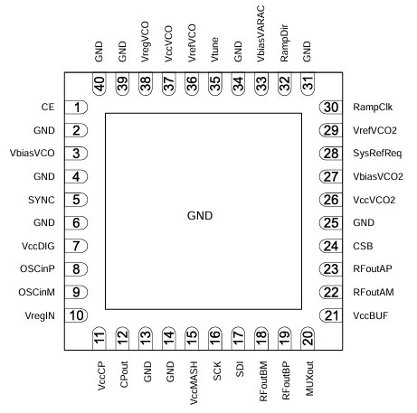
Here is the “Pin Functions” table from page 7 in markdown format:
| PIN NO. | PIN NAME | I/O | DESCRIPTION |
|---|---|---|---|
| 1 | CE | Input | Chip enable input. Active HIGH powers on the device. |
| 2, 4, 25, 31, 34, 39, 40 | GND | Ground | VCO ground. |
| 3 | VbiasVCO | Bypass | VCO bias. Requires a 10-µF capacitor connected to VCO ground. Place close to pin. |
| 5 | SYNC | Input | Phase synchronization pin. Has programmable threshold. |
| 6, 14 | GND | Ground | Digital ground. |
| 7 | VccDIG | Supply | Digital supply. TI recommends bypassing with decoupling capacitor to digital ground. |
| 8 | OSCinP | Input | Reference input clock (+). High-impedance self-biasing pin. Requires AC-coupling capacitor. (0.1 µF recommended) |
| 9 | OSCinM | Input | Reference input clock (–). High impedance self-biasing pin. Requires AC-coupling capacitor. (0.1 µF recommended) |
| 10 | VregIN | Bypass | Input reference path regulator output. Requires a 1-µF capacitor connected to ground. Place close to pin. |
| 11 | VccCP | Supply | Charge pump supply. TI recommends bypassing with decoupling capacitor to charge pump ground. |
| 12 | CPout | Output | Charge pump output. TI recommends connecting C1 of loop filter close to pin. |
| 13 | GND | Ground | Charge pump ground. |
| 15 | VccMASH | Supply | Digital supply. TI recommends bypassing with decoupling capacitor to digital ground. |
| 16 | SCK | Input | SPI clock. High impedance CMOS input. 1.8-V to 3.3-V logic. |
| 17 | SDI | Input | SPI data. High impedance CMOS input. 1.8-V to 3.3-V logic. |
| 18 | RFoutBM | Output | Differential output B (–). Requires a pullup (typically 50-Ω resistor) connected to Vcc as close to the pin as possible. Can be used as an output signal or SYSREF output. |
| 19 | RFoutBP | Output | Differential output B (+). Requires a pullup (typically 50-Ω resistor) connected to Vcc as close to the pin as possible. Can be used as an output signal or SYSREF output. |
| 20 | MUXout | Output | Multiplexed output pin — lock detect, readback, diagnostics, ramp status. |
| 21 | VccBUF | Supply | Output buffer supply. TI recommends bypassing with decoupling capacitor to RFout ground. |
| 22 | RFoutAM | Output | Differential output A (–). Requires connecting a 50-Ω resistor pullup to Vcc as close to the pin as possible. |
| 23 | RFoutAP | Output | Differential output A (+). Requires connecting a 50-Ω resistor pullup to Vcc as close to the pin as possible. |
| 24 | CSB | Input | SPI latch. Chip Select Bar. High-impedance CMOS input. 1.8-V to 3.3-V logic. |
| 26 | VccVCO2 | Supply | VCO supply. TI recommends bypassing with decoupling capacitor to VCO ground. |
| 27 | VbiasVCO2 | Bypass | VCO bias. Requires a 1-µF capacitor connected to VCO ground. |
| 28 | SysRefReq | Input | SYSREF request input for JESD204B support. |
| 29 | VrefVCO2 | Bypass | VCO supply reference. Requires a 10-µF capacitor connected to VCO ground. |
| 30 | RampClk | Input | Input pin for ramping mode that can be used to clock the ramp in manual ramping mode or as a trigger input. |
| 32 | RampDir | Input | Input pin for ramping mode that can be used to change ramp direction in manual ramping mode or as a trigger input. |
| 33 | VbiasVARAC | Bypass | VCO Varactor bias. Requires a 10-µF capacitor connected to VCO ground. |
| 35 | Vtune | Input | VCO tuning voltage input. |
| 36 | VrefVCO | Bypass | VCO supply reference. Requires a 10-µF capacitor connected to VCO ground. |
| 37 | VccVCO | Supply | VCO supply. Recommend bypassing with decoupling capacitor to ground. |
| 38 | VregVCO | Bypass | VCO regulator node. Requires a 1-µF capacitor connected to ground. |
Example Use case
FMCW Radar Systems (Frequency Modulated Continuous Wave):
The Scenario: Modern radar systems require a signal source that can rapidly and accurately sweep across a range of frequencies (a “chirp”) to determine the distance and velocity of an object.
How the LMX2594 is used: The LMX2594 features built-in automatic and manual frequency ramping functions. A designer can program the IC to automatically generate up to two segments of a frequency ramp without needing constant microcontroller intervention. Coupled with its fast VCO calibration speed (<20 µs), the IC can rapidly sweep frequencies, making it a perfect signal source for high resolution FMCW radar.
Applications of LMX2594
- 5G and mm Wave wireless infrastructure
- Test and measurement equipment
- Radar
- MIMO (Multiple Input Multiple Output) systems
- Phased array antennas and beamforming
- High speed data converter clocking (supporting JESD204B standards)
Summary
The LMX2594 delivers ultra-low phase noise and wide frequency coverage for demanding microwave applications. It is ideal for advanced RF, radar, and communication system designs.
Continue Learning Frequency Synthesizers
Resources on synthesizing complex frequencies for RF transmission, covering design, settling time, and Direct Digital Synthesis (DDS).