
AD8302 Gain/Phase Detector IC Pin Diagram, Circuit and Applications
Advertisement
The AD8302 is a gain and phase detector IC capable of simultaneously measuring amplitude ratio and phase difference between two RF input signals. It is widely used in antenna tuning, phased-array systems, vector measurement instruments, impedance analysis, and RF communication equipment. This article covers its pin diagram, operating principle, circuit design, features, and applications.
Key features of AD8302
- Wide Frequency Range: Measures Gain/Loss and Phase from low frequencies up to 2.7 GHz.
- Wide Input Dynamic Range: Accommodates input signals from –60 dBm to 0 dBm in a 50 Ω system.
- High Accuracy Scaling:
- Gain Measurement: Scaled to 30 mV/dB with a typical nonlinearity of < 0.5 dB.
- Phase Measurement: Scaled to 10 mV/Degree over a 0°–180° range with a typical nonlinearity of < 1 Degree.
- Versatile Operation Modes: Can be used in Measurement, Controller, or Level Comparator modes.
- Integrated Components: Features dual closely matched demodulating logarithmic amplifiers (60 dB range each) and a precise multiplier type phase detector.
- Broadband Envelope: Small signal envelope bandwidth from DC to 30 MHz (can be reduced via external filter capacitors).
- Power & Reference: Operates on a single supply voltage of 2.7 V to 5.5 V and provides a stable, loadable 1.8 V reference voltage output.
AD8302 Pin Diagram
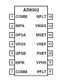
Here’s a look at the AD8302 pin diagram:
| Pin number | Description | Function |
|---|---|---|
| 1 | COMM | Device Common. Connect to low impedance ground. |
| 2 | INPA | High Input Impedance to Channel A. Must be ac-coupled. |
| 3 | OFSA | A capacitor to ground at this pin sets the offset compensation filter corner and provides input decoupling. |
| 4 | VPOS | Voltage Supply (VS), 2.7 V to 5.5 V |
| 5 | OFSB | A capacitor to ground at this pin sets the offset compensation filter corner and provides input decoupling. |
| 6 | INPB | Input to Channel B. Same structure as INPA |
| 7 | COMM | Device Common. Connect to low impedance ground. |
| 8 | PFLT | Low Pass Filter Terminal for the Phase Output |
| 9 | VPHS | Single-Ended Output Proportional to the Phase Difference between INPA and INPB. |
| 10 | PSET | Feedback Pin for Scaling of VPHS Output Voltage in Measurement Mode. Apply a setpoint voltage for controller mode. |
| 11 | VREF | Internally Generated Reference Voltage (1.8 V Nominal) |
| 12 | MSET | Feedback Pin for Scaling of VMAG Output Voltage Measurement Mode. Accepts a set point voltage in controller mode. |
| 13 | VMAG | Single-Ended Output. Output voltage proportional to the decibel ratio of signals applied to INPA and INPB |
| 14 | MFLT | Low Pass Filter Terminal for the Magnitude Output |
Example Circuit : AD8302 for gain/phase measurement
As shown in the figure-2, AD8302 is used to measure gain and insertion phase of device under test (DUT) which is marked as “Black Box”. It can either be amplifier or mixer.
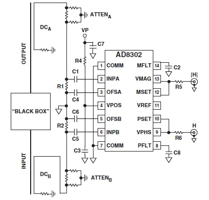
Directional couplers are used to sample the input signal going into the DUT and the output signal coming out of it. Attenuators are applied to these sampled signals to ensure they fall within the AD8302’s optimal dynamic range (ideally centered around –30 dBm).
The AD8302 compares the two signals and outputs a voltage representing the exact gain/loss and phase shift. If the amplifier starts to compress at high power levels (AM-AM distortion) or exhibits excess phase shifts (AM-PM conversion), the AD8302 outputs these deviations in real-time.
Applications of AD8302
- RF/IF Power Amplifier (PA) Linearization
- Precise RF Power Control
- Remote System Monitoring and Diagnostics
- Return Loss/VSWR (Voltage Standing Wave Ratio) Measurements
- Log Ratio Function for AC Signals
Summary
The AD8302 simplifies simultaneous gain and phase measurements with high accuracy. It is widely used in RF test equipment, communication systems, and antenna measurement applications.