
What is CD4001 NOR Gate IC? Pin Diagram and Applications
By RF Wireless Expert Team
Advertisement
The CD4001 is a CMOS quad two-input NOR gate integrated circuit designed for implementing digital logic functions. It offers low power consumption, high input impedance, and reliable operation in logic, timing, and control applications.
Key features of CD4001
- Logic Function: Performs the Boolean NOR function.
- CMOS Technology: Constructed with monolithic N and P-channel enhancement mode transistors.
- Buffered Outputs: Improves transfer characteristics by providing very high gain.
- Symmetrical Drive: Equal source and sink current capabilities.
- Broad Voltage Range: 5V, 10V, and 15V parametric ratings (Operating range from 3 Vdc to 15 Vdc).
- Low Power TTL Compatibility: Fan out of 2 driving 74L compatibility, or 1 driving 74LS.
- ESD Protection: All inputs are protected against static discharge with diodes to Vdd and Vss.
- Low Leakage: Maximum input leakage is 1 µA at 15V over the full temperature range.
CD4001 Pin Diagram
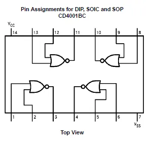
| Pin Number | Pin Name | Description |
|---|---|---|
| 1 | Input 1A | Data Input A for Gate 1 |
| 2 | Input 1B | Data Input B for Gate 1 |
| 3 | Output 1J | NOR Output for Gate 1 |
| 4 | Output 2J | NOR Output for Gate 2 |
| 5 | Input 2B | Data Input B for Gate 2 |
| 6 | Input 2A | Data Input A for Gate 2 |
| 7 | Ground / Negative Power Supply | |
| 8 | Input 3A | Data Input A for Gate 3 |
| 9 | Input 3B | Data Input B for Gate 3 |
| 10 | Output 3J | NOR Output for Gate 3 |
| 11 | Output 4J | NOR Output for Gate 4 |
| 12 | Input 4B | Data Input B for Gate 4 |
| 13 | Input 4A | Data Input A for Gate 4 |
| 14 | Positive Power Supply (3V to 15V) |
Example Use Case : SR (Set-Reset) Latch Memory Element
-
Scenario: You need a simple hardware switch debounce circuit or a basic 1-bit memory latch to hold a state (like a fault flag) until it is manually cleared.
-
How to use CD4001BC :
- Because the CD4001BC contains four independent NOR gates, you can use two of them to create an SR Latch:
- Connect the Output (Pin 3) of Gate 1 to Input (Pin 5) of Gate 2.
- Connect the Output (Pin 4) of Gate 2 to Input (Pin 2) of Gate 1.
- The remaining free inputs (Pin 1 and Pin 6) become your Set and Reset inputs.
- By applying a HIGH signal to the “Set” pin, the latch will flip and hold its state on the outputs even after the input goes back LOW. Applying a HIGH to the “Reset” pin clears the state.
This utilizes the device’s exact Boolean function described in datasheet to store a piece of digital information.
Applications of CD4001
- General Logic Implementation: Creating boolean logic combinations in digital circuits.
- Signal Inversion: By tying both inputs of a single gate together, it can act as a standard NOT gate (Inverter).
- CMOS to TTL Interfacing: Because it features low power TTL compatibility (can drive 74L/74LS loads), it is useful for bridging standard CMOS circuits to TTL components.
Summary
CD4001 contains four NOR gates for implementing various digital logic circuits and control systems.