
What is CD4011 NAND Gate IC? Pin Diagram and Applications
By RF Wireless Expert Team
Advertisement
The CD4011 is a CMOS integrated circuit containing four independent two-input NAND gates. It is commonly used in digital logic circuits, counters, flip-flops, oscillators, timing circuits, and embedded electronic systems due to its low power consumption and high noise immunity.
Key features of CD4011
- Logic Function: Performs the Boolean NAND function.
- Buffered Outputs: Designed with buffered outputs to improve transfer characteristics by providing very high gain.
- CMOS Construction: Monolithic complementary MOS integrated circuit utilizing N- and P-channel enhancement mode transistors.
- Symmetrical Drive: Equal source and sink current capabilities conforming to standard B series output drive.
- Low Power TTL Compatibility: Can drive up to two 74L loads or one 74LS load directly.
- Wide Operating Voltage: Parametric ratings at 5V, 10V, and 15V (Operating range from 3V to 15V).
- ESD Protection: All inputs are protected against static discharge via internal diodes to Vdd and Vss.
- Low Leakage: Maximum input leakage current of just 1 µA at 15V over the full temperature range.
CD4011 Pin Diagram
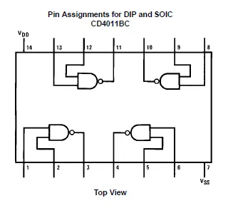
| Pin Number | Pin Name | Description |
|---|---|---|
| 1 | Input 1A | Data Input A for Gate 1 |
| 2 | Input 1B | Data Input B for Gate 1 |
| 3 | Output 1J | NAND Output for Gate 1 |
| 4 | Output 2J | NAND Output for Gate 2 |
| 5 | Input 2B | Data Input B for Gate 2 |
| 6 | Input 2A | Data Input A for Gate 2 |
| 7 | Ground / Negative Power Supply | |
| 8 | Input 3A | Data Input A for Gate 3 |
| 9 | Input 3B | Data Input B for Gate 3 |
| 10 | Output 3J | NAND Output for Gate 3 |
| 11 | Output 4J | NAND Output for Gate 4 |
| 12 | Input 4B | Data Input B for Gate 4 |
| 13 | Input 4A | Data Input A for Gate 4 |
| 14 | Positive Power Supply (3V to 15V DC) |
Example Use Case : Active-Low SR Latch (Hardware Debouncer)
-
Scenario: You need a simple circuit to debounce a physical Single Pole Double Throw (SPDT) switch. Physical switches “bounce” mechanically when flipped, sending dozens of rapid on/off spikes to a microcontroller, which causes errors.
-
Solution : Wire two of the independent NAND gates on the CD4011BC to create an Active-Low Set-Reset (SR) Latch.
Applications of CD4011
- Universal Logic Implementation: Because NAND is a “universal gate,” the CD4011 can be used to construct any other type of logic gate (AND, OR, NOT, XOR, etc.).
- Signal Inversion: By connecting both inputs of a single gate together, it functions as a NOT gate (Inverter).
- Astable and Monostable Multivibrators: Commonly used with resistors and capacitors to build simple clock oscillators, timers, and pulse generators.
- CMOS to TTL Bridging: Utilizing its low power TTL compatibility to interface different logic families.
Summary
CD4011 integrates four NAND gates in one package for implementing digital logic functions efficiently.