
ADL5513 RF Detector IC Pin Diagram, Circuit and Applications
Advertisement
The ADL5513 is a broadband RF detector IC designed for accurate measurement of RF signal power and envelope characteristics. It is widely used in wireless transmitters, receivers, RF instrumentation, signal monitoring, and communication test equipment. This article explains its pin diagram, working, circuit design, specifications, and applications.
Key features of ADL5513
- Wide Bandwidth: 1 MHz to 4 GHz.
- High Dynamic Range: 80 dB dynamic range (+/- 3 dB error) and 74 dB (+/- 1 dB error) that remains constant over frequency.
- High Sensitivity: –70 dBm.
- Excellent Stability: +/- 0.5 dB stability over a –40°C to +85°C temperature range (programmable/adjustable via the TADJ pin).
- Fast Response Time: 21 ns / 20 ns (fall/rise) pulse response time, enabling RF burst detection to pulse rates beyond 50 MHz.
- Operating Temperature Range: –40°C to +125°C.
- Power Efficiency: Single-supply operation from 2.7 V to 5.5 V at 31 mA. Features a power down mode that drops current consumption to 200 μA (1 mW at 5 V).
- Output Modes: Can be used in both Measurement Mode (linear in dB output) and Controller Mode (error amplifier output for control loops) with low noise output (VOUT). Package: Small footprint 3 mm × 3 mm, 16-lead LFCSP.
ADL5513 Pin Diagram
Here’s a look at the ADL5513 pin diagram:
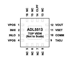
| Pin No. | Pin Name | Type | Function |
|---|---|---|---|
| 1 | VPOS | Power | Positive supply voltage input (2.7 V to 5.5 V). |
| 2 | INHI | RF Input | AC-coupled RF input. Accepts the RF signal whose power is to be measured. |
| 3 | INLO | RF Input | RF common (return) for the INHI input. AC-coupled. |
| 4 | VPOS | Power | Positive supply voltage. Connect to the same supply as Pin 1. |
| 5 | NC | — | No internal connection. Leave open or connect to the ground plane if desired. |
| 6 | NC | — | No internal connection. |
| 7 | NC | — | No internal connection. |
| 8 | NC | — | No internal connection. |
| 9 | TADJ | Analog Input | Temperature compensation adjustment input. Also functions as the power-down (PWDN) control. Applying a voltage near VPOS − 0.3 V disables the device. |
| 10 | COMM | Ground | Device ground reference. Connect directly to PCB ground. |
| 11 | VSET | Analog Input | Setpoint input for controller mode. In RSSI (measurement) mode, connect VSET to VOUT. |
| 12 | VOUT | Analog Output | Logarithmic detector output voltage proportional to the RF input power. Also acts as the error amplifier output in controller mode. |
| 13 | NC | — | No internal connection. |
| 14 | CLPF | Analog | Loop filter capacitor connection. An external capacitor sets the video bandwidth and output response time. |
| 15 | NC | — | No internal connection. |
| 16 | NC | — | No internal connection. |
Example Use Case : Constant Power Operation (Automatic Gain Control)
The ADL5513 can be configured in Controller Mode to act as the error amplifier in an Automatic Gain Control (AGC) loop. This is highly useful in transmit topologies where a transmitter card is driving a High Power Amplifier (HPA), and the output power must be held perfectly stable over a broad temperature or input power range.
Applications of ADL5513
- RF transmitter power amplifier linearization and gain/power control.
- Power monitoring in radio link transmitters.
- RSSI (Received Signal Strength Indicator) measurement in base stations, WLAN, WiMAX, and RADAR systems.
Summary
The ADL5513 combines high accuracy with broadband operation for RF signal detection. It is ideal for power monitoring and wireless communication systems.