
PE4259 SPDT RF Switch IC: Pin Diagram & Circuit Guide
Advertisement
PE4259 is a high frequency SPDT RF switch IC used to route radio frequency signals between different signal paths. Its single pole double throw configuration allows one RF port to be switched between two other ports, making it useful for antenna selection, transmitter/receiver switching, test equipment, RF signal routing, and wireless communication systems.
Key features of PE4259
- Broad Frequency Range: Operates from 10 MHz to 3.0 GHz (3000 MHz).
- High Power Handling: Features a typical input 1 dB compression point (P1dB) of +33.5 dBm, making it suitable for high power signal routing.
- Low Insertion Loss: 0.35 dB at 1000 MHz and 0.5 dB at 2000 MHz.
- High Isolation: Provides 30 dB of isolation at 1000 MHz.
- Flexible Control Logic: Features on-board CMOS control logic that can be driven via a single pin or complementary pin interface.
- Low Power/Voltage Operation: Can operate with a minimum power supply voltage of just 1.8V (3.0V nominal).
- High ESD Tolerance: Rated for 2 kV HBM (Human Body Model).
- Ultra-Small Footprint: Packaged in a compact 6-lead SC-70 package.
- UltraCMOS Technology: Manufactured on a sapphire substrate, combining the high RF performance of GaAs with the economy and integration of standard CMOS.
PE4259 Pin Diagram
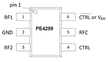
Pin Details (6-Lead SC-70 Package)
| Pin Number | Pin Name | Description |
|---|---|---|
| 1 | RF1 | RF Port 1.(Note: Must be DC blocked with an external series capacitor or held at 0 VDC). |
| 2 | GND | Ground Connection. Traces must be physically short and connected to the ground plane for best RF performance. |
| 3 | RF2 | RF Port 2. (Note: Must be DC blocked with an external series capacitor or held at 0 VDC). |
| 4 | CTRL | Switch Control Input. CMOS logic level input used to toggle the switch path. |
| 5 | RFC | RF Common Port. (Note: Must be DC blocked with an external series capacitor or held at 0 VDC). |
| 6 | or VDD | Dual-Function Pin. • Single-pin control mode: Connect to a nominal 3V DC supply (). • Complementary-pin control mode: Acts as the complementary CMOS control signal to Pin 4 (CTRL). |
Example Use Case : 2.4 GHz T/R Switch with Single-Pin Control
Scenario: It is required to design 2.4 GHz wireless transceiver for an IoT device with single antenna. This antenna need to be shared between Power Amplifier (PA) for transmitting and Low Noise Amplifier (LNA) for receiving.
Implemetation : This will be implemented using PE4259 with appropriate connections with the help of microcontroller.
Applications of PE4259
- Transmit/Receive (T/R) Switching in portable wireless devices.
- Antenna Diversity Routing in ISM band transceivers (e.g., 900 MHz, 2.4 GHz).
- RF Signal Routing in cellular and mobile communication nodes.
- Test and Measurement Equipment requiring reliable, high power solid state switching.
Summary
PE4259 provides controlled RF signal routing between multiple paths using an SPDT configuration. Its compact implementation is useful for antenna selection, transmitter/receiver switching, RF test systems, and wireless equipment.