
CC1101 RF Transceiver IC: Pinout, Circuit & Applications
Advertisement
CC1101 is a low power sub GHz RF transceiver IC designed for wireless communication in the ISM frequency bands. It integrates an RF transmitter, receiver, frequency synthesizer, modem, and digital interface in a compact device, making it suitable for applications such as wireless sensors, remote controls, home automation, telemetry, and low data rate embedded communication.
Key features of CC1101
-
RF & Analog Performance:
- Broad Frequency Support: Operates in the 300-348 MHz, 387-464 MHz, and 779-928 MHz bands (covering 315/433/868/915 MHz ISM/SRD bands).
- High Sensitivity: Down to -116 dBm at 0.6 kBaud (433 MHz) and -112 dBm at 1.2 kBaud (868 MHz).
- Programmable Output Power: Up to +12 dBm across all supported frequencies.
- Versatile Modulation: Supports 2-FSK, 4-FSK, GFSK, MSK, as well as OOK and flexible ASK shaping.
- Programmable Data Rate: Ranging from 0.6 kbps to 600 kbps.
-
Low-Power Capabilities:
- Ultra Low Sleep Current: 200 nA in sleep mode.
- Fast Startup: 240 μs transition from sleep to RX/TX mode.
- Wake-on-Radio (WOR): Allows automatic, low power RX polling without microcontroller (MCU) interaction.
-
Digital Features:
- Packet Handling: Extensive on-chip hardware support for sync word detection, address checking, flexible packet lengths, and automatic CRC calculation.
- FIFOs: Separate 64-byte RX and TX data FIFOs to enable burst mode data transmission and offload MCU processing.
- Link Qualifiers: Digital RSSI output, Clear Channel Assessment (CCA), Carrier Sense (CS) and Link Quality Indicator (LQI).
CC1101 Pin Diagram
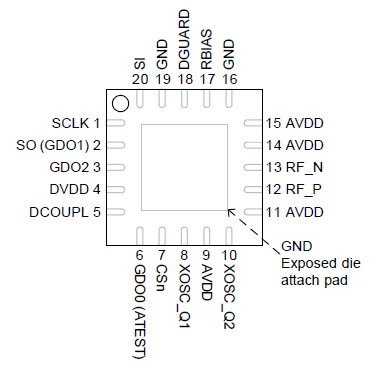
| Pin # | Pin Name | Type | Description |
|---|---|---|---|
| 1 | SCLK | Digital Input | SPI configuration interface, clock input. |
| 2 | SO (GDO1) | Digital Output | SPI configuration interface, data output. Can also be a general output pin. |
| 3 | GDO2 | Digital Output | General-purpose digital output (Test signals, FIFO status, Clock output, etc.). |
| 4 | DVDD | Power | 1.8V - 3.6V digital power supply for I/Os and digital core. |
| 5 | DCOUPL | Power | 1.6V - 2.0V digital power supply output for decoupling (do not use to power external devices). |
| 6 | GDO0 (ATEST) | Digital I/O | General-purpose digital output pin (similar to GDO2) / analog test I/O. |
| 7 | CSn | Digital Input | SPI configuration interface, chip select. |
| 8 | XOSC_Q1 | Analog I/O | Crystal oscillator pin 1 (or external clock input). |
| 9 | AVDD | Power | 1.8V - 3.6V analog power supply connection. |
| 10 | XOSC_Q2 | Analog I/O | Crystal oscillator pin 2. |
| 11 | AVDD | Power | 1.8V - 3.6V analog power supply connection. |
| 12 | RF_P | RF I/O | Positive RF input to LNA (RX) / Positive RF output from PA (TX). |
| 13 | RF_N | RF I/O | Negative RF input to LNA (RX) / Negative RF output from PA (TX). |
| 14 | AVDD | Power | 1.8V - 3.6V analog power supply connection. |
| 15 | AVDD | Power | 1.8V - 3.6V analog power supply connection. |
| 16 | GND | Ground | Analog ground connection. |
| 17 | RBIAS | Analog I/O | External bias resistor connection for reference current. |
| 18 | DGUARD | Power | Power supply connection for digital noise isolation. |
| 19 | GND | Ground | Ground connection for digital noise isolation. |
| 20 | SI | Digital Input | SPI configuration interface, data input. |
Example Use Case : Wireless Automatic Meter Reading
Scenario: A city is deploying battery powered smart water meters to homes. Because the meters run on batteries and must last 10+ years without maintenance, extreme low power is critical.
Solution : The CC1101 can be paired with a low power microcontroller (like MSP430). The CC1101 spends 99.9% of its time in its 200 nA SLEEP mode.
Instead of keeping the receiver constantly on or requiring the MCU to wake up the radio, the CC1101’s internal WOR timer automatically wakes the receiver up for brief milliseconds to check for an incoming “data request” signal from a passing utility truck or local neighborhood gateway.
When a request is detected via the Carrier Sense and a valid sync word is matched, the CC1101 wakes up the MCU. The MCU pushes the water usage data into the CC1101’s 64 byte TX FIFO, which bursts the data over the air at a high data rate (e.g. 250 kbps) using GFSK modulation in the 868 MHz band.
Once the payload transmits, the radio controller automatically flushes the FIFOs and returns the CC1101 to its ultra-low power sleep state, preserving battery life.
Applications of CC1101
- Ultra low power wireless applications in 315/433/868/915 MHz ISM/SRD bands
- Wireless sensor networks
- Automatic Meter Reading
- Wireless alarm and security systems
- Home and building automation
- Industrial monitoring and control
- Wireless MBUS systems
Summary
CC1101 provides a compact, low power solution for sub-GHz wireless communication. Its integrated RF transceiver and modem simplify wireless sensor, telemetry, remote control and home automation designs.