
LMX2572 Wideband PLL IC: Pinout, Circuit & Applications
Advertisement
LMX2572 is a high performance wideband frequency synthesizer and PLL IC used to generate precise RF and microwave frequencies from a reference clock. It incorporates a programmable phase locked loop, frequency divider and multiplier functions, and an integrated VCO, making it suitable for local oscillators, clock generation, wireless infrastructure, test equipment, radar and other high frequency systems.
Key features of LMX2572
- Wide Output Frequency Range: 12.5 MHz to 6.4 GHz (without using an internal doubler).
- Low Power Consumption: Consumes only 75 mA from a single 3.3-V supply.
- Excellent Phase Noise Performance:
- –106-dBc/Hz at 100-kHz offset with a 6.4-GHz carrier.
- PLL figure of merit: –232 dBc/Hz.
- PLL normalized 1/f noise: –123.5 dBc/Hz.
- High Resolution Fractional-N Divider: 32-bit fractional-N divider allowing very fine frequency steps.
- Spur Reduction: Programmable input multiplier to remove integer boundary spurs.
- Advanced Synchronization: Supports output phase synchronization across multiple devices.
- JESD204B Support: Can generate or repeat SYSREF signals with programmable delay.
- Modulation & Sweeping Support: Built-in support for ramp/chirp functions and FSK direct digital modulation (discrete level and pulse-shaping).
- Outputs: Two programmable output power level differential outputs.
- Fast VCO Calibration: Calibrates in < 20 µs.
LMX2572 Pin Diagram
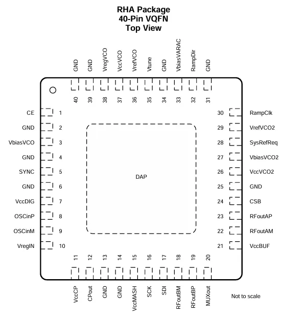
| Pin Name | Pin No. | I/O | Description |
|---|---|---|---|
| CE | 1 | Input | Chip enable. High impedance CMOS input. 1.8-V to 3.3-V logic. Active HIGH powers on the device. |
| CPout | 12 | Output | Charge pump output. Place C1 of loop filter close to this pin. |
| CSB | 24 | Input | SPI latch. High impedance CMOS input. 1.8-V to 3.3-V logic. |
| DAP | — | Ground | RF ground. |
| GND | 2, 4, 25, 31, 34, 39 | Ground | VCO ground. |
| GND | 6, 14, 40 | Ground | Digital ground. |
| GND | 13 | Ground | Charge pump ground. |
| MUXout | 20 | Output | Multiplexed output pin. Configurable between lock detect and register readback. |
| OSCinM | 9 | Input | Reference input clock (–). High impedance self-biasing pin. Requires AC-coupling. |
| OSCinP | 8 | Input | Reference input clock (+). High impedance self-biasing pin. Requires AC-coupling. |
| RampClk | 30 | Input | Ramp trigger in automatic ramping mode or ramp clock in manual ramping mode. High impedance CMOS input. 1.8-V to 3.3-V logic. |
| RampDir | 32 | Input | Ramp trigger in automatic ramping mode or ramp segment selection in manual ramping mode. High impedance CMOS input. 1.8-V to 3.3-V logic. |
| RFoutAM | 22 | Output | Differential output A (–). Low impedance output. Requires AC-coupling. |
| RFoutAP | 23 | Output | Differential output A (+). Low impedance output. Requires AC-coupling. |
| RFoutBM | 18 | Output | Differential output B (–). Low impedance output. Requires AC-coupling. Configurable between RF output or SYSREF output. |
| RFoutBP | 19 | Output | Differential output B (+). Low impedance output. Requires AC-coupling. Configurable between RF output or SYSREF output. |
| SCK | 16 | Input | SPI clock. High impedance CMOS input. 1.8-V to 3.3-V logic. |
| SDI | 17 | Input | SPI data. High impedance CMOS input. 1.8-V to 3.3-V logic. |
| SYNC | 5 | Input | Phase synchronization trigger. Configurable to accept CMOS input (1.8-V to 3.3-V logic) or differential input. |
| SysRefReq | 28 | Input | SYSREF request for JESD204B support. Configurable to accept CMOS input (1.8-V to 3.3-V logic) or differential input. |
| VbiasVARAC | 33 | Bypass | VCO Varactor bias. Connect a 10-µF decoupling capacitor to VCO ground. |
| VbiasVCO | 3 | Bypass | VCO bias. Connect a 470-nF (X7R) decoupling capacitor to VCO ground as close to this pin as possible. |
| VbiasVCO2 | 27 | Bypass | VCO bias. Connect a 100-nF (X7R) decoupling capacitor to VCO ground. |
| VccBUF | 21 | Supply | Supply for output buffers. Connect a 0.1-µF decoupling capacitor to RF ground. |
| VccCP | 11 | Supply | Supply for charge pump. Connect a 0.1-µF decoupling capacitor to charge pump ground. |
| VccDIG | 7 | Supply | Digital power supply. Connect a 0.1-µF decoupling capacitor to digital ground. |
| VccMASH | 15 | Supply | Digital power supply. Connect a 1-µF decoupling capacitor to digital ground. |
| VccVCO | 37 | Supply | Supply for VCO. Connect a 1-µF decoupling capacitor to VCO ground. |
| VccVCO2 | 26 | Supply | Supply for VCO. Connect a 1-µF decoupling capacitor to VCO ground. |
| VrefVCO | 36 | Bypass | VCO supply reference. Connect a 10-µF decoupling capacitor to VCO ground. |
| VrefVCO2 | 29 | Bypass | VCO supply reference. Connect a 10-µF decoupling capacitor to VCO ground. |
| VregIN | 10 | Bypass | Input reference path regulator output. Connect a 1-µF decoupling capacitor to RF ground as close to this pin as possible. |
| VregVCO | 38 | Bypass | VCO regulator node. Connect a 10-nF decoupling capacitor to VCO ground. |
| Vtune | 35 | Input | VCO tuning voltage input. Connect a 1.5-nF or more capacitor to VCO ground. See External Loop Filter for details. |
Example Use Case : Synthesizing 4-level GFSK Modulation for a Wireless Radio
The LMX2572 is utilized to generate 4-level Gaussian Frequency Shift Keying (GFSK) modulation for wireless communication.
In the setup, A 100 MHz reference oscillator (XO) is fed into the “OSCin” pins. The base PLL components (Doubler, Multiplier, Pre-R, Post-R, CHDIV) are configured to set the nominal “RFout” carrier frequency to 490 MHz.
The device is put into FSK SPI FAST mode. Rather than utilizing pre-stored frequency deviations, the system’s data generator streams SPI data (via the SCK, SDI, and CSB pins) continuously.
The continuous bit stream writes dynamically update the fractional numerator in real time, effectively oversampling the data to create a smooth, pulse shaped Gaussian transition between the four discrete frequency deviations
This method allows a simple RF synthesizer to achieve arbitrary level FSK and analog FM type modulations digitally, eliminating the need for an external I/Q modulator and reducing overall system power and footprint.
Applications of LMX2572
- Test and measurement equipment
- Digital 2-way radios
- Low power radio communication systems
- Satellite communication
- Wireless microphones
- Proprietary wireless connectivity
- MIMO & RADAR systems
- High speed data converter clocking (using JESD204B capabilities)
Summary
LMX2572 provides programmable high frequency synthesis for generating precise RF and microwave signals. Its integrated PLL and VCO functions can reduce external circuitry and support applications including local oscillators, wireless infrastructure, radar, and test equipment.
Continue Learning Frequency Synthesizers
Resources on synthesizing complex frequencies for RF transmission, covering design, settling time, and Direct Digital Synthesis (DDS).