
AD9361 RF Agile Transceiver: Pinout, Circuit & Applications
Advertisement
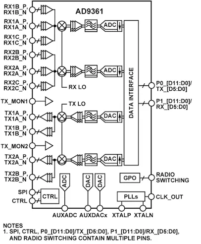
AD9361 is a highly integrated RF agile transceiver IC designed for software defined radio and wideband wireless communication systems. It integrates programmable transmit and receive signal paths, RF frequency synthesis, analog to digital and digital to analog conversion, and configurable baseband interfaces, making it suitable for applications such as SDR platforms, cellular infrastructure, wireless instrumentation and defense communication systems.
Key features of AD9361
- Highly Integrated Transceiver: 2 × 2 (dual transmit, dual receive) direct conversion architecture with integrated 12-bit DACs and ADCs.
- Wide Frequency Range: Transmitter (TX) operates from 47 MHz to 6.0 GHz; Receiver (RX) operates from 70 MHz to 6.0 GHz.
- Flexible Bandwidth: Tunable channel bandwidth ranging from less than 200 kHz up to 56 MHz.
- Duplex Support: Supports both Frequency Division Duplex (FDD) and Time Division Duplex (TDD) operations.
- High Performance Receiver: State-of-the-art noise figure (2 dB at 800 MHz LO) with independent automatic gain control (AGC), real-time manual gain control, and dc/quadrature correction.
- High Linearity Transmitter: Achieves an Error Vector Magnitude (EVM) of ≤−40 dB and an ultralow noise floor (≤−157 dBm/Hz).
- Integrated Components: Fully integrated fractional-N synthesizers (2.4 Hz max LO step size), internal VCOs, and loop filters.
- Digital Interface: Configurable CMOS/LVDS digital interface to easily connect with baseband processors.
AD9361 Pin Diagram
Following are the summarized pin descriptions including their corresponding pin numbers from Table 13 of datasheet.
AD9361 Pin Descriptions
| Category | Mnemonic | Pin Number(s) | Short Description |
|---|---|---|---|
| RF Inputs | RX1A_N/P to RX1C_N/P | M1, M2, H1, J1, K1, L1 | Receive channel 1 differential inputs (A, B, C). |
| RX2A_N/P to RX2C_N/P | A1, A2, E1, F1, C1, D1 | Receive channel 2 differential inputs (A, B, C). | |
| RF Outputs | TX1A_N/P, TX1B_N/P | M7, M8, M9, M10 | Transmit channel 1 differential outputs (A, B). |
| TX2A_N/P, TX2B_N/P | A7, A8, A9, A10 | Transmit channel 2 differential outputs (A, B). | |
| TX_MON1, TX_MON2 | M5, A5 | Transmit power monitor inputs. | |
| Data Ports | P0_D[11:0] / TX_D[5:0] | D7 to D11, E7 to E12, F8 | Digital Data Port 0 / LVDS TX data bus. |
| P1_D[11:0] / RX_D[5:0] | H8, J7 to J12, K7 to K11 | Digital Data Port 1 / LVDS RX data bus. | |
| Clocks & Sync | DATA_CLK_P, DATA_CLK_N | G11, H11 | Receive data clock output. |
| FB_CLK_P, FB_CLK_N | F10, G10 | Feedback clock input (TX data timing reference). | |
| RX_FRAME_P, RX_FRAME_N | G8, G7 | RX digital data framing output. | |
| TX_FRAME_P, TX_FRAME_N | G9, H9 | TX digital data framing input. | |
| CLK_OUT | J6 | Output clock (buffered or divided). | |
| XTALP, XTALN | M11, M12 | Crystal connections for reference frequency. | |
| RX_EXT_LO_IN | G1 | External RX local oscillator input. | |
| TX_EXT_LO_IN | A12 | External TX local oscillator input. | |
| SYNC_IN | H5 | Digital clock synchronization input. | |
| SPI & Control | SPI_ENB, SPI_CLK, SPI_DI, SPI_DO | K6, J5, J4, L6 | SPI bus interface pins. |
| CTRL_IN[3:0] | C5, C6, D6, D5 | Real-time control inputs (e.g., manual gain). | |
| CTRL_OUT[7:0] | D4, E4 to E6, F4 to F6, G4 | Programmable real-time control outputs. | |
| ENABLE | G6 | State machine control input. | |
| TXNRX | H4 | State machine control signal (RX vs TX direction). | |
| EN_AGC | G5 | Manual control input for AGC. | |
| RESETB | K5 | Asynchronous device reset. | |
| Auxiliary | AUXDAC1, AUXDAC2 | B3, C3 | Auxiliary DAC outputs. |
| AUXADC | L5 | Auxiliary ADC input. | |
| GPO_3 to GPO_0 | B4 to B7 | 3.3 V general-purpose logic outputs. | |
| Power | VDD_INTERFACE | H12 | Digital I/O supply (1.2 V to 2.5 V). |
| VDD_GPO | B8 | Supply for AUXDAC and GPO pins (2.5 V to 3.3 V). | |
| VDDD1P3_DIG | F12 | 1.3 V Digital supply input. | |
| VDDAx (Analog Supplies) | A11, B9, B10, D2, D3, E2, E3, F2, G3, J3, K3, K4 | Various 1.3 V analog, RF, and VCO supply inputs. | |
| Ground | VSSA (Analog Ground) | A4, A6, B1, B2, B12, C2, C7-C12, F3, H2, H3, H6, J2, K2, L2, L3, L7-L12, M4, M6 | Analog ground connections. |
| VSSD (Digital Ground) | D12, F7, F9, F11, G12, H7, H10, K12 | Digital ground connections. | |
| Misc | TX_VCO_LDO_OUT | B11 | Transmit VCO LDO output (needs bypass cap). |
| RX_VCO_LDO_OUT | G2 | Receive VCO LDO output (needs bypass cap). | |
| RBIAS | L4 | Bias input reference (requires 14.3 kΩ resistor). | |
| TEST/ENABLE | C4 | Test input (tie to ground for normal operation). | |
| NC | A3, M3 | No connect. |
Example Use Case
The primary use case for the AD9361 is acting as the core radio frequency transceiver for a localized 4G microcell or femtocell (such as a private corporate cellular network or dense urban cell tower).
Applications of AD9361
- Point to point communication systems.
- Femtocell, picocell and microcell base stations.
- General purpose radio systems.
Summary
AD9361 integrates major RF transmit and receive functions into a highly configurable transceiver, reducing external component requirements. Its wideband and programmable architecture makes it valuable for SDR, wireless infrastructure, instrumentation and advanced communication systems.