What is RF Sputtering: 5 Advantages and Disadvantages
Advertisement
RF sputtering is a thin film deposition process that uses radio frequency plasma to deposit insulating and conductive materials onto substrates with high precision. Its advantages include excellent film uniformity and compatibility with dielectric materials, while its disadvantages include slower deposition rates, higher equipment costs, and complex process control.
Working operation of RF Sputtering
Here’s a look at a typical RF sputtering system:
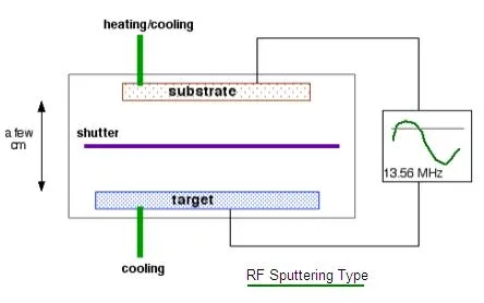
Key Features of the System:
- RF Source Frequency: 13.56 MHz
- RF Peak-to-Peak Voltage: 1000 V
- Electron Densities: 109 to 1011 Cm-3
- Chamber Pressure: 0.5 to 10 mTorr
RF sputtering involves alternating positive and negative cycles. During the positive cycle, electrons are drawn to the cathode, creating a negative bias. In the negative cycle, ion bombardment continues. Crucially, this method prevents ion buildup on insulating targets by avoiding a constant negative voltage on the cathode.
Advantages of RF Sputtering
- Improved Film Quality & Step Coverage: RF sputtering generally produces films with better quality and step coverage compared to evaporation techniques.
- Versatile Material Deposition: It’s well-suited for depositing a wide range of materials, including insulators, metals, alloys, and composites. It particularly excels with insulating targets.
- Reduced Charge-Up Effects & Arcing: The use of an AC RF source at 13.56 MHz helps to minimize charge-up effects and arcing. This is because the electric field sign at every surface inside the plasma chamber changes with the RF signal.
- Efficient Operation at Low Pressures: RF sputtering can operate at low pressures (1 to 15 mTorr) while sustaining plasma, leading to higher efficiency.
- Applicable to Any Film Type: This technique can be used to sputter virtually any type of film.
- Advanced RF Diode Sputtering: Recently developed RF diode sputtering techniques offer improved performance compared to standard RF sputtering.
Disadvantages of RF Sputtering
- Low Deposition Rates: Deposition rates can be quite slow for certain materials when using RF sputtering.
- Complex RF Power Application: Applying RF power isn’t straightforward. It necessitates expensive power supplies and additional impedance matching circuitry.
- Stray Magnetic Field Leakage: Leakage from ferromagnetic targets can disrupt the sputtering process. While sputter guns with strong permanent magnets can mitigate this, they increase the system’s cost.
- Heat Generation: Most of the incident energy on the target is converted into heat, which needs to be removed, adding complexity to the system.
- Difficult Uniform Deposition on Complex Structures: Achieving uniform deposition on complex structures like turbine blades can be challenging.
- Challenges with Thick Coatings: Producing high-performance thick coatings can be difficult due to higher internal residual stress levels.
Summary
RF sputtering has become an important fabrication technique for semiconductor devices, optical coatings, sensors, and advanced materials because it produces high quality thin films with excellent consistency. Its processing advantages outweigh its higher operational costs in applications requiring precision and material versatility.