TTL vs LVTTL: Understanding the Differences
Advertisement
This article explores the differences between TTL (Transistor-Transistor Logic) and LVTTL (Low Voltage TTL), covering their voltage levels, advantages, and disadvantages.
Introduction
The first TTL IC, the 7400, was developed in 1965 and became known as “Standard TTL.” TTL families utilize transistors to perform fundamental logic operations. TTL devices often serve as “glue logic,” connecting more complex components within a digital system. The basic TTL logic circuit is a NAND gate, which internally uses BJTs (Bipolar Junction Transistors).
TTL | Transistor-Transistor Logic
- It’s one of the most common I/O standards.
- TTL typically operates from a +5V or 3.3V power supply.
- TTL employs three primary output configurations: open collector, totem pole, and three-state (or tristate) outputs.
- Standard TTL family ICs include: 7404, 74S86, and 74ALS161.
- Binary logic “1”: Represented by a voltage between 2.4V and 5V (VCC), and must be more than 2V.
- Binary logic “0”: Represented by a voltage between 0V and 0.8V, and must be less than 0.8V.
The following are typical characteristics of the TTL logic family:
- Basic gate used: NAND
- Fanout: 10
- Power per gate: 1-22 mW
- Noise immunity: Very good
- Noise margin: 0.3 (High), 0.5 (Low)
- (propagation delay): 1.5 to 33 ns
- Output drive current: Asymmetric: High state: 0.4 to 2 mA, Low state: 8 to 20 mA

TTL and CMOS interfacing
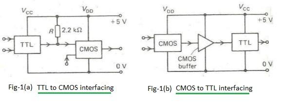
The figure above illustrates interfacing between TTL and CMOS logic.
Advantages of TTL
- Low power consumption, higher output swing, low implementation cost, fast switching speeds, etc.
- Totem pole TTL output configurations offer high fanout, low power dissipation, and high operating speeds. Totem pole outputs do not require external pull-up resistors.
Disadvantages of TTL
- Consumes more power than CMOS, making it less suitable for battery-powered devices.
- Fanout (component density) is less than CMOS.
- Poorer noise immunity compared to CMOS.
- In totem pole configurations, outputs of two gates cannot be directly tied together.

TTL and LVTTL voltage levels
LVTTL | Low Voltage TTL
- LVTTL is a JEDEC standard referencing the input signal to ground.
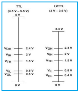
- The output switching range is 0.4V to 2.4V for the 3.3V LVTTL version.
- The output switching range is 0.4V to 2.2V for the 2.5V LVTTL version.
The following are the receiver input and driver output specifications of LVTTL:
LVTTL and TTL Driver Output
-
At a low logic level, the maximum driver output voltage () is 0.4V for both LVTTL and TTL. The minimum output voltage is GND (ground).
-
At a high logic level, the minimum output voltage () is 2.4V for both LVTTL and TTL, and the maximum is Vcc, which is 3.3V for LVTTL and 5V for TTL.
LVTTL and TTL Receiver Input
-
For a low logic level, the maximum input voltage () is 0.8V for both LVTTL and TTL; the minimum input voltage to the receiver is GND (ground).
-
For a high logic level, the minimum input voltage () is 2V for TTL/LVTTL, and the maximum receiver input voltage is Vcc, i.e., 3.3V for LVTTL and 5V for TTL.
Advertisement
 RF
RF


