C Band RF Transceiver Design and Block Diagram
Advertisement
This page describes the design and development of a C band RF transceiver, detailing its various modules as per the RF transceiver block diagram. An RF Transceiver typically consists of:
- RF Up Converter
- RF Down Converter
- 10MHz OCXO (Oven Controlled Crystal Oscillator)
- RF Synthesizer
- Local Oscillator
- RF Power Divider
- IF Power Divider
- M & C (Monitoring and Control) Card
- Power Supply
The RF transceiver is a major module in wireless systems, essentially comprising a transmitter and a receiver. The C band RF Transceiver finds use in VSAT (Very Small Aperture Terminal) systems or Earth stations, providing wireless connectivity with satellites from the ground.
VSAT is used for voice and data call connections by users in both hilly and flat terrains.
RF Transceiver Specifications
The following specifications are considered in the C band RF transceiver design described here:
Transmitter Part Specifications:
- Input frequency: 52 to 88 MHz
- Output frequency: 5925 to 6425 MHz
- RF frequency selection: In steps of approximately 1 MHz
- Conversion Gain: 20 dB minimum
- Gain Flatness: +/- 1 dB over the entire band
- Gain Variation: +/-1 dB over temperature range of 0°C to 50°C
- Gain Adjustment: 10 dB
- Input power level: -5 to -25dBm
- Spurious and harmonics level: Better than -40 dBc
- 1 dB compression point: Better than +3dBm
Receiver Part Specifications:
- Input frequency: 3.7 to 4.2 GHz
- Output frequency: 52 to 88 MHz
- RF frequency selection: In steps of approximately 1 MHz
- Conversion Gain: 40 dB minimum
- Input level: -40dBm to -85dBm
- Gain Flatness: +/- 1 dB over the entire band of 36MHz
- Gain Variation: +/-1 dB over temperature range of 0°C to 50°C
- Gain Adjustment: 10 dB
- Noise Figure: Better than 14dB
- Image rejection: Better than -50dBc
- Spurious and harmonics level: Better than -40 dBc
RF Transceiver Block Diagram
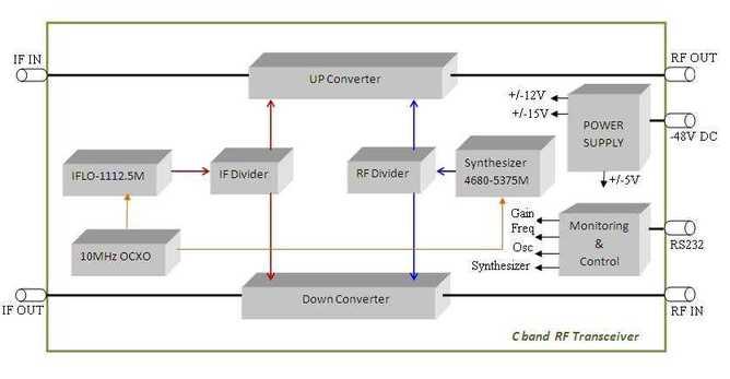
The primary function of the RF Transceiver is to convert modulated IF (Intermediate Frequency) signals into RF (Radio Frequency) signals and vice versa. It interfaces with the modem (baseband part) on one side and with the PA/LNA (Power Amplifier/Low Noise Amplifier) on the other. Due to its location in the VSAT system, it’s often referred to as the Outdoor Unit (ODU). It mainly comprises an Up Converter and a Down Converter.
As shown in the figure below, the Up Converter converts the modulated IF IN (70+/-18 MHz) into the modulated RF OUT (5925-6425MHz). The Down Converter converts the modulated RF IN (3700-4200) MHz to IF OUT (70+/-18 MHz).

Figure-1 : C Band RF Transceiver Block Diagram
As shown in the block diagram, the RF Transceiver consists of modules which include:
- Up Converter
- Down Converter
- OCXO
- Synthesizer
- Local Oscillator
- RF Divider
- IF Divider
- M & C card
- Power Supply
Guide to C band RF Transceiver design
As mentioned, the RF Transceiver consists of two major modules: the RF Up Converter and the Down Converter.
- The RF Up Converter converts the lower frequency to a higher frequency.
- The RF Down Converter converts the higher frequency to a lower frequency.
This design of RF frequency converters is carried out using discrete RF components. Microstrip lines are etched on a PCB for soldering the RF components.
RF Up Converter and RF Down Converter
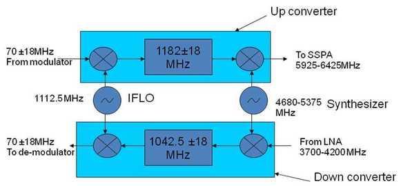
As shown in the figure below, the RF Up Converter converts modulated IF data in the frequency band of 52-88 MHz to C band. This is done using mixers and filters, employing a dual conversion approach.
In the first conversion, 70MHz beats with 1112.5MHz LO (Local Oscillator), producing sum and difference frequencies. The sum frequencies are then picked up and passed through a filter of 1182.5+/- 18 MHz. This 1182.5 band of frequencies beats with a 4680-5375 MHz RF synthesizer, producing a C band of about 5925-6425 MHz. Two RF mixers in the up converter and down converter follow a heterodyne architecture design.
For the RF down converter design, LNA signal frequencies of about 3.7GHz band are converted to IF frequencies of about 70MHz. This is again achieved with appropriate mixers/filters. In the first conversion step, the 3.7GHz band is converted to a 1042.5MHz band after beating with a synthesizer. This same 1042.5MHz band is converted to a 70MHz IF signal after beating with a fixed IF Local Oscillator of 1112.5MHz frequency.

10MHz OCXO
This RF oscillator serves as the reference for both the IFLO and the synthesizer in the RF Transceiver. A small power divider circuit is designed to split the sinusoidal power output of the oscillator into two paths. One path is fed as input to the IF Local Oscillator, and the other is fed as input to the RF Synthesizer. This module is designed by purchasing the required RF components, including a 10 MHz crystal oscillator of OCXO type, and developing a microstrip-based board.
Radio Frequency Synthesizer
The synthesizer is used to change the RF frequency of operation in the RF Transceiver used for VSAT. The RF synthesizer here operates from 4680 to 5375 MHz, and the frequency can be set in steps of 1 MHz. There are many manufacturers of RF synthesizer modules which one can buy for the development or can be designed and developed.
Local Oscillator
The RF Local Oscillator generates a fixed frequency and cannot be changed, unlike the RF Synthesizer. An RF local oscillator value of 1112.5MHz is used in this design.
RF Power Divider
The RF divider module is designed using a microstrip concept. Various methods are available to develop an RF divider; the Wilkinson power divider is a popular choice. The RF divider splits the RF output of the synthesizer into two paths: one is used as input to the mixer for RF up conversion, and the other is used as input to the mixer for RF down conversion.
IF Power Divider
The IF divider module is also designed using a microstrip concept. Various methods are available to design and develop this module. The IF divider splits the IF output of the Local Oscillator into two paths: one is used as input to the mixer for IF up conversion, and the other is used as input to the mixer for IF down conversion.
M & C Card
The Monitoring and Control card is used to monitor and control various parameters such as power level (Gain), RF carrier frequency, oscillator reference adjustment, synthesizer frequency control, and more. The M & C card is composed of a microcontroller, RAM, EPROM, RS232 interface, DAC/ADC, and more. The RS232 interface is used to remotely control various parameters from a PC. Sometimes RS485 is used due to its multi-drop and long-distance advantages.
Power Supply
A very stable power supply is crucial for achieving better phase noise, a requirement for interworking with the satellite network. The power supply here converts -48V DC to other DC voltages such as +/-12, +/-15, +/-5, which are fed to other modules in the RF Transceiver. The power supply should have minimal ripple to obtain good performance.
Conclusion
The design steps outlined in this article on RF transceiver design can also be applied to RF transceivers on other frequency bands such as L band, Ku band, K band and Ka bands.
Advertisement
 RF
RF


