
What is Schottky Barrier Diode: Advantages and Disadvantages
Advertisement
A Schottky barrier diode is a semiconductor diode that uses a metal-semiconductor junction to achieve fast switching and low forward voltage drop. Its advantages include high switching speed and low power loss, while its disadvantages include higher reverse leakage current and lower reverse voltage capability than conventional PN junction diodes.
Schottky Barrier Diode Structure and Circuit working operation
Schottky diodes are constructed using N-type silicon with a thin layer of metal deposited on top. In this configuration, the semiconductor acts as the cathode, and the metal functions as the anode. Common anode materials include nickel, chromium, and aluminum, although gold and other metals are also used.
Schottky diodes typically have an ON-voltage of about 0.3V, compared to 0.7V for a standard P-N junction diode.
Figure-1 depicts a Schottky diode and its equivalent circuit.
As shown, it’s made of a thin silicon substrate with an epitaxially grown n-type active layer (approximately 2 microns thick). A thin SiO2 layer is thermally grown over the active layer. The metal-semiconductor junction is formed by depositing metal over the SiO2.
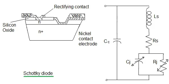
When the device is forward biased, major carriers are easily injected from the heavily doped n-semiconductor material into the metal.
Conversely, when reverse biased, the barrier height becomes too high for electrons to cross, preventing conduction.
Benefits or Advantages of Schottky Barrier Diodes
-
Wide Application Range: These diodes are suitable for applications where other diode types are less effective. Examples include RF mixers, detector diodes, solar cells, and voltage clamping devices.
-
Low Turn-On Voltage: They offer a low turn-on voltage, typically between 0.2 and 0.3 Volts.
-
No Recovery Time: Unlike P-N junction diodes, Schottky diodes have virtually no recovery time when switching between conducting and non-conducting states.
-
Fast Recovery Time: This characteristic results in a small amount of stored charge, making them ideal for high-speed switching applications.
-
Low Junction Capacitance: Schottky diodes have low junction capacitance. The resulting structure occupies a small area after wire point contact with the silicon.
-
High-Frequency Operation: They can operate at higher frequencies compared to PN junction diodes and are often used as fast switches at microwave frequencies.
-
Higher I0 Current: The saturation current (I0) of a Schottky diode is much larger compared to a PN junction diode, dependent on the barrier height (fB).
Drawbacks or Disadvantages of Schottky Barrier Diodes
-
Low Voltage Operation: They typically operate at lower voltages (around 50V) compared to P-N junction diodes. They can’t withstand significantly higher reverse voltages without breaking down. This limits their application in high voltage situations.
-
Higher Reverse Current: Schottky diodes exhibit a relatively higher reverse current (leakage current), which can be a concern in certain circuit designs.
Summary
Schottky barrier diodes are widely used in power supplies, RF circuits, switching regulators, and high speed electronics because of their excellent efficiency and fast response. Their electrical advantages improve performance, although leakage current and voltage limitations should be considered during circuit design.