What is NMOS and PMOS Transistors : Key differences explained
Advertisement
NMOS and PMOS are two fundamental types of MOSFET transistors used in digital and analog circuits. NMOS (N-channel MOSFET) transistors conduct when supplied with a positive gate voltage, while PMOS (P-channel MOSFET) transistors conduct with a negative gate voltage. These complementary transistors are used in electronic circuits to control the flow of electrical current. They are fundamental building blocks in digital logic circuits and analog signal processing circuits. In CMOS circuits, they work together to create efficient digital logic gates. Understanding their key differences helps in CMOS design, power efficiency, switching speed and semiconductor applications.
NMOS structure and diagram
-
The symbol for an NMOS transistor consists of an arrow pointing towards the gate, indicating the direction of electron flow when the transistor is ON.
-
As shown, it consists of three layers of semiconductor materials viz. source, drain, and gate. A thin insulating layer of oxide separates the gate from the semiconductor material. The gate terminal is typically made of conductive material like metal or polysilicon.
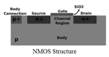 Figure-1 depicts NMOS structure diagram.
PMOS structure and diagram
-
The symbol for a PMOS transistor is a circle with an arrow pointing away from the gate, indicating the direction of hole flow when the transistor is ON.
-
A PMOS transistor has a similar structure to NMOS but with opposite polarity. As shown, it consists of source, drain, and gate terminals, but in PMOS, holes are the majority carriers. The gate-source voltage controls the flow of holes between the source and drain.
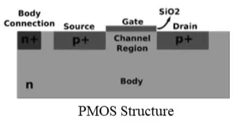 Figure-2 depicts PMOS structure diagram.
Characteristics
The circuit symbols and V-I characteristics of NMOS and PMOS transistors are as follows.
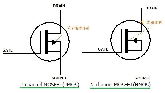 Figure-3 depicts symbols of N-channel MOSFET (NMOS) and P-channel MOSFET (PMOS).
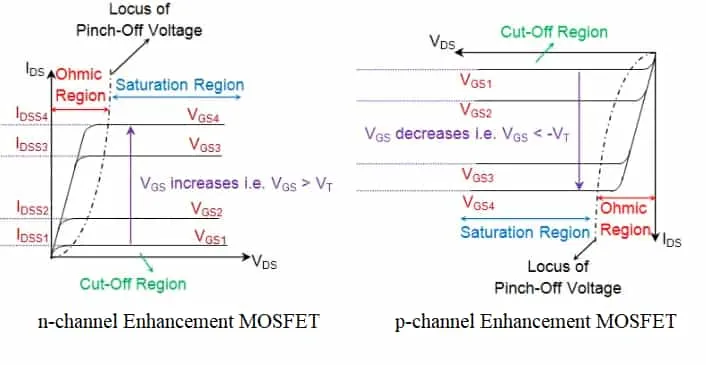 Figure-4 depicts NMOS and PMOS enhancement MOSFET characteristics.
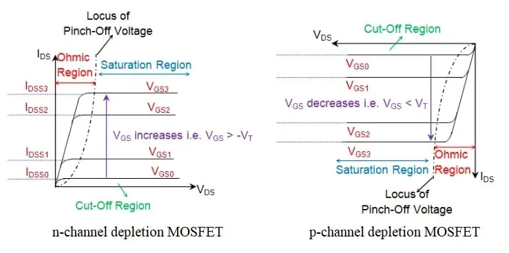 Figure-5 depicts NMOS and PMOS depletion MOSFET characteristics.
What is the difference between NMOS and PMOS
The following table compares PMOS vs NMOS MOSFET types with respect to various parameters.
| Parameters | PMOS (P-Channel MOSFET) | NMOS (N-Channel MOSFET) |
|---|---|---|
| Carrier type | Majority carriers are holes (Positive) | Majority carriers are electrons (negative) |
| Operation | Conducts when Vgs < Vth (Gate < Source) | Conducts when Vgs > Vth (Gate > Source) |
| Symbol | Circular symbol with arrow pointing away from gate | Arrow symbol pointing towards the gate |
| Voltage levels | Positive gate source voltage (Vgs) | Negative gate source voltage (Vgs) |
| Logic level | Positive voltage represents logical ‘0’ | Positive voltage represents logical ‘1’ |
| Switching speed | Generally slower than NMOS | Generally faster than PMOS |
| Noise immunity | More noise immunity due to slower switching | Less noise immunity due to faster switching |
| Power consumption | Consumes more power when ON | Consumes less power when ON |
| Power supply polarity | Often used in circuits with negative power supplies | Often used in circuits with positive power supplies |
| Common use cases | Voltage level translators, analog circuitry | Digital logic gates, amplifiers in audio applications |
Summary
We can derive following difference between NMOS and PMOS transistors.
- P-channel is much easier and cheaper to produce compared to an N-channel MOSFET device.
- The N-channel MOSFET has a high packing density. This makes it faster for switching applications due to smaller junction areas and low inherent capacitances.
- N-channel MOSFET is smaller for the same complexity compared to P-channel MOSFET.
- Drain resistance of P-channel MOSFET is 3 times higher than an identical N-channel MOSFET device.
- N-channel MOSFET has a high false turn-on possibility compared to a P-channel device. This is due to positively charged contaminants.
- For a given drain current rating, P-channel MOSFET occupies a larger area compared to N-channel MOSFET. This is due to the fact that electron mobility is 2.5 times greater than the mobility of a hole.
In short, NMOS and PMOS transistors have distinct carrier types and operate with opposite polarities. They are often used together to create complementary logic gates in digital circuits, taking advantage of their differences to minimize power consumption and improve performance.