
MMIC Fabrication Techniques
Advertisement
Monolithic Microwave Integrated Circuits (MMICs) are integrated circuits where all active and passive elements, components, and connections are fabricated simultaneously on a single substrate. This is achieved through various deposition techniques, some of which are described below.
The primary MMIC fabrication techniques include:
- Diffusion
- Ion Implantation
- Epitaxial Growth
- Lithography
- Photo Etching
- Deposition
MMIC fabrication necessitates careful selection of the dielectric substrate material and the fabrication process itself. Substrate materials for MMICs are chosen based on their function:
- Substrate Materials: For mounting electronic devices (e.g., Alumina, Ferrite, GaAs, Sapphire).
- Conductor Materials: For printing patterns and creating ground planes (e.g., Aluminium, Copper, Gold, Silver).
- Dielectric Materials: For capacitors and blockers (e.g., SiO, Si3N4, Al2O3, Ta2O5, SiO2).
- Resistive Materials: For bias networks, attenuators, and terminations (e.g., Cr, NiCr, Ta, Ti).
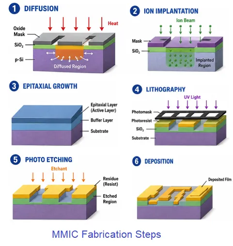
1. Diffusion
It is a high temperature thermal process used to alter the electrical properties of a semiconductor wafer by introducing specific impurity atoms, known as dopants. During this step, the wafer is placed in a heavily heated furnace filled with a dopant rich gas, causing the impurity atoms to physically migrate into the crystal lattice through a concentration gradient.
While this technique was a staple in early silicon manufacturing, it is somewhat limited in modern Monolithic Microwave Integrated Circuit (MMIC) fabrication because it lacks the microscopic depth precision required for high frequency RF transistors. However, it is still occasionally employed to form deep, non-critical contact regions or to manipulate bulk substrate characteristics where absolute nanoscale precision is not the primary concern.
2. Ion Implantation
It is a highly precise, mechanical doping method where impurity atoms are electrically charged and accelerated through a high voltage magnetic field before being shot directly into the semiconductor substrate at room temperature. Because the penetration depth and concentration of these atomic “bullets” can be strictly controlled by adjusting the accelerator’s voltage, this process allows engineers to create incredibly shallow and exact doping profiles.
This level of precision is absolutely critical in MMIC fabrication, as ultra-fast microwave transistors require strictly defined conductive channels to handle high frequency electron flow. After the ions are embedded, the wafer undergoes a brief thermal annealing process to repair any structural damage to the crystal lattice and properly activate the newly introduced dopants.
3. Epitaxial Growth
Epitaxial growth is the highly controlled process of depositing a flawless, new layer of crystalline material directly on top of the bare wafer, ensuring the new layer perfectly mimics and extends the underlying crystal lattice structure. Utilizing advanced vacuum chamber techniques like Molecular Beam Epitaxy (MBE) or Metal Organic Chemical Vapor Deposition (MOCVD), engineers can build these layers one atom at a time.
In the realm of MMICs, epitaxy is arguably the most vital fabrication step because it enables the creation of heterojunctions—stacking disparate materials like Gallium Nitride (GaN) and Aluminum Gallium Nitride (AlGaN). The microscopic boundary where these two epitaxial materials meet forms a frictionless, high speed pathway known as a 2D Electron Gas, which is the foundational engine powering high performance microwave and millimeter wave amplifiers.
4. Lithography
It acts as the photographic blueprinting phase of fabrication, where the complex geometric patterns of the microwave circuit are physically transferred onto the wafer’s surface. The substrate is first coated with a light sensitive polymer called photoresist, and then exposed to intense ultraviolet light (or a focused electron beam) passed through a specialized stencil known as a mask.
This exposure chemically alters specific regions of the resist, allowing a developer solution to wash away the unwanted areas and leave behind a temporary, protective stencil of the circuit.
For high frequency MMICs, traditional optical lithography is often replaced by Electron Beam (E-beam) lithography, which provides the atomic level precision necessary to draw the ultra-thin, sub-micron transistor gates required to effectively process Terahertz and high gigahertz RF signals.
5. Photo Etching
It is a subtractive manufacturing process that carves the physical circuit elements out of the semiconductor material by permanently removing any areas not shielded by the lithographic photoresist.
While wet etching relies on liquid chemical baths to dissolve material quickly, modern MMIC fabrication leans heavily on dry etching techniques, such as Reactive Ion Etching (RIE), which uses a vacuum sealed plasma gas to bombard the wafer. This microscopic sandblasting effect carves straight down into the substrate with perfectly vertical walls, allowing engineers to isolate densely packed RF transistors into distinct “mesas” and drill precise via holes entirely through the wafer to connect components to a backside ground plane, a feature vital for minimizing RF interference and grounding high frequency circuits.
6. Deposition
It is an additive process used to construct the intricate wiring and passive components of the MMIC by blanketing the wafer with thin films of conductive metals or insulating dielectrics.
Through techniques like Physical Vapor Deposition (PVD), where metals are evaporated or sputtered in a vacuum to condense on the wafer, or Chemical Vapor Deposition (CVD) for growing insulating layers, the actual microwave circuitry comes to life.
In MMIC manufacturing, deposition is heavily used to lay down thick layers of high conductivity metals; most commonly gold, due to its exceptional RF performance and resistance to oxidation to form the microstrip transmission lines, thin film resistors, spiral inductors, and capacitors that directly integrate the active transistors into a complete, functioning microwave integrated circuit.
Summary
The manufacturing of Monolithic Microwave Integrated Circuits (MMICs) relies on a highly controlled, sequential combination of semiconductor fabrication techniques, each specially optimized to handle ultra-high frequency RF signals.
Continue Learning MMIC
- MMIC : Key Advantages and Disadvantages
- Hybrid vs. Monolithic Microwave IC (MMIC): Key Differences, Biasing and Manufacturers