What is Indium Phosphide (InP) : Advantages and Disadvantages
Advertisement
Indium Phosphide (InP) is a semiconductor material known for its high electron mobility and excellent optical properties. It is widely used in photonics, fiber-optic communications, RF devices, and high-speed electronics. Advantages include superior high frequency performance, while disadvantages include higher manufacturing costs and material fragility.
Key Features of Indium Phosphide (InP)
- Indium phosphide is a binary semiconductor composed of indium and phosphorus.
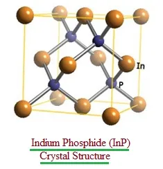
- It possesses a face-centered cubic crystal structure, similar to GaAs and other III-V semiconductors. (See Figure 1)
- The preparation of indium phosphide typically occurs at 400°C through the reaction of white phosphorus and indium iodide.
- InP is used in high-frequency electronics, especially at high power levels.
- When combined with InGaAs, it can form pseudomorphic HBTs (Heterojunction Bipolar Transistors) that can operate at frequencies up to 604 GHz.
- It’s also crucial in manufacturing optoelectronic devices and photonic ICs for telecommunication systems.
Here are some key properties of Indium Phosphide (InP):
- Band gap: 1.34 eV
- Structure: Zinc blende
- Electron mobility: 5400 cm2/(V*s) at 300 K
- Thermal conductivity: 0.7 W/(cm*K) at 300 K
- Refractive index (nD): 3.1 (infrared)
Benefits or Advantages of Indium Phosphide (InP)
- Superior Electron Velocity: InP boasts a much higher electron velocity compared to silicon (Si) and gallium arsenide (GaAs), approximately 5 times greater.
- Direct Band Gap: This property makes InP efficient for light emission and absorption.
- Lower Base Sheet Resistance: Offers about 20 times lower resistance.
- Higher Base Electron Diffusivity: Exhibits about 5 times higher electron diffusivity.
- Higher Breakdown at Same fT: Demonstrates about 4 times higher breakdown.
Drawbacks or Disadvantages of Indium Phosphide (InP)
- Limited Scaling: Currently, production is only scaled to around ~1 µm.
- Emitter Issues: Suffers from large emitters and poor emitter contact.
- Low Current Density: Exhibits a low current density, approximately 2 mA/µm2.
- High Collector Capacitance: Has a high collector capacitance.
- Non-Planar Device with Low Yield: Manufacturing processes often result in non-planar devices and lower yields.
- Low Integration Scales: Integration scales are generally low.
Summary
Indium Phosphide enables high speed optical and RF device performance. Advantages include exceptional frequency response and optical efficiency, while disadvantages include costly fabrication and handling challenges.