DC vs. RF Sputtering: Key Differences Explained
Advertisement
Sputtering is a versatile thin-film deposition technique widely used in industries like electronics, optics, and materials science. Among the various sputtering methods, DC (Direct Current) and RF (Radio Frequency) sputtering stand out due to their distinct working principles and applications. While DC sputtering is often employed for conductive materials, RF sputtering offers versatility with both conductive and insulating materials. This article dives into the core differences between RF and DC sputtering, highlighting their working principles, advantages, limitations, and typical use cases.
What is Sputtering?
Sputtering is a highly versatile vacuum coating system used for the deposition of various coating materials.
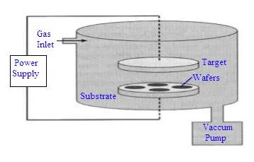
Plasma gas is used to knock atoms out of the target, resulting in atom deposition on wafers. Higher pressure generates better coverage, and the excess energy of metal ions helps to increase surface mobility (i.e., movement of atoms on the surface).
DC Sputtering
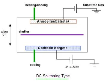
- In DC sputtering, the power source is DC (Direct Current).
- DC power is usually preferred for electrically conductive target materials as it is easy to control.
- Chamber pressure is typically 1 to 100 mTorr.
- It is a cheaper technique when dealing with large quantities of large substrates.
- In this technique, positively charged sputtering gas is accelerated towards the target. This results in the ejection of atoms, which are then deposited on the substrate.
RF Sputtering
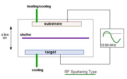
- In RF sputtering, the power source is AC (Alternating Current). Instead of DC voltage to the cathode, RF at about 13.56 MHz is applied.
- RF peak-to-peak voltage is 1000 V, electron densities are to , and chamber pressure is 0.5 to 10 mTorr.
- RF power is suitable for all materials but is most commonly used for depositing films from dielectric target materials.
- The deposition rate is lower compared to DC sputtering.
- It is used for smaller substrate sizes due to the high cost factor of RF power supplies.
- RF sputtering consists of two processes:
- First cycle: The target material is negatively charged, causing polarization of atoms. The sputtering gas atoms are attracted towards the source, where they knock out source atoms. Here, source atoms and ionized gas ions remain at the target surface due to polarization of the target.
- Second cycle: The target is positively charged, causing the ejection of gas ions and source atoms due to reverse polarization. These are accelerated toward the substrate, and deposition occurs.
Difference between RF and DC Sputtering
The following table summarizes the core differences between RF and DC sputtering techniques.
| Features | DC Sputtering | RF Sputtering |
|---|---|---|
| Sputtering type | Magnetron only | Magnetron or diode |
| Target materials | Conductive only | All the targets |
| Power Source | Uses a direct current (DC) power source. | Uses a radio frequency (RF) power source, typically 13.56 MHz. |
| Material Suitability | Suitable only for conductive materials. | Suitable for both conductive and insulating materials. |
| Target Charging | Cannot sputter insulating targets due to target charging. | Prevents target charging through alternating RF electric fields. |
| Complexity | Simple setup and operation. | More complex setup due to the RF power source and matching network. |
| Cost | Lower equipment cost. | Higher equipment cost due to RF generators. |
| Deposition Rate | Generally higher deposition rates for conductive materials. | Deposition rates are often lower than DC sputtering. |
| Applications | Commonly used for metal films and conductive coatings. | Ideal for dielectric, insulating, and mixed-material films. |
| Plasma Generation | Relies on a steady plasma for material removal. | Alternating RF fields sustain a stable plasma even with insulating materials. |
| Maintenance | Easier maintenance due to simpler components. | Requires more frequent tuning and complex maintenance. |
| Efficiency | Higher efficiency with conductive materials. | Lower efficiency but more versatile material handling. |
| Sputtering rate | 100% of DC | 20% of DC, no magnetron |
| Campaign length (anode loss) | Good | Excellent |
Conclusion
Both DC and RF sputtering are essential thin-film deposition techniques, each suited to specific material requirements and applications. DC sputtering excels in simplicity and efficiency for conductive materials, while RF sputtering’s versatility makes it ideal for a wider range of materials, including insulators. Understanding these differences ensures the right method is chosen for a given application, optimizing performance and quality.