 RF
RFP-I-N vs. Schottky vs. Avalanche Photodiode: A Comparison
Advertisement
This page compares P-I-N diodes, Schottky Barrier photodiodes, and Avalanche photodiodes, highlighting the basic differences between them. All these diodes function as optical detectors, also known as photodetectors.
The function of a photodiode is to convert a light signal into either a voltage or current, depending on the mode of operation. Photodiodes are designed to operate under reverse bias conditions. They have two modes of operation: the photoelectric effect and photocurrent. Different materials are used in manufacturing photodiodes based on the wavelength of operation, as detailed in the table below.
| Material | EM Spectrum | Wavelength (nm) |
|---|---|---|
| Silicon | 190 to 1100 | |
| Germanium | 400 to 1700 | |
| Indium Gallium Arsenide | 800 to 2600 | |
| Lead(II) Sulfide | < 1000 to 3500 |
The diodes designed for use as photodiodes typically employ a P-I-N junction rather than a P-N junction. They are packaged with a window or fiber connection to allow light to reach the sensitive part of the device.
P-I-N Diode
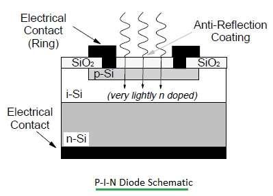
Figure 1 illustrates the structure of a P-I-N diode. As shown, it features a very lightly doped layer, referred to as the intrinsic zone, between the P and N doped layers. This is why the device is known as a P-I-N diode instead of a P-N diode. The I-layer has a very small amount of dopant and acts as a very wide depletion layer.
Typically, a P-I-N diode operates at any wavelength shorter than the cutoff wavelength. When light falls on the diode, the energy of the absorbed photon must be sufficient to promote an electron across the bandgap; otherwise, it will not be absorbed. The material will absorb photons of any energy higher than the bandgap energy. P-I-N diodes operate at different wavelengths depending on the materials used in their construction. Common wavelength bands include 500 to 1000 nm, 1250 to 1400 nm, and 1500 to 1600 nm.
Schottky Barrier Photodiode
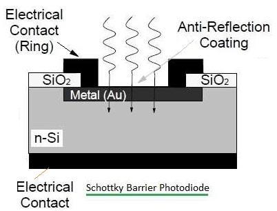
Sometimes it is impossible to realize P-I-N diodes for a given wavelength band. Moreover, the performance of such diodes may not be sufficient for use as optical detectors. In these situations, Schottky barrier photodiodes are employed.
Figure 2 depicts the structure of a Schottky Barrier Photodiode. As shown, a thin metal layer replaces either the P-region or N-region of the diode. Hence, it is known as a “metal-semiconductor diode”. Depending on the semiconductor and metal used, a barrier is formed at the interface of these two materials. This barrier results in the bending of the bands. By applying voltage, the bands can be bent more or less. In this region of band bending, electron-hole pairs can be easily separated.
Avalanche Photodiode
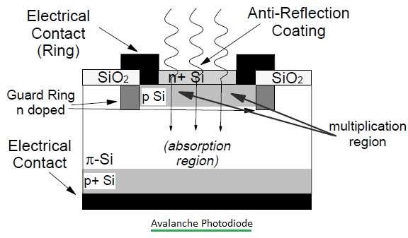
One way to increase the sensitivity of an optical receiver is through amplification. An Avalanche Photodiode is used to amplify the signal in addition to the optical detection process. The device operation is based on the “Avalanche Effect”. In the avalanche effect, a highly accelerated electron excites another electron through “impact ionization”.
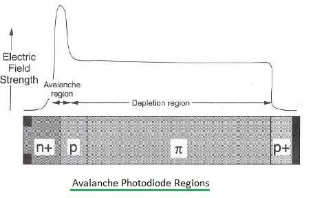
As shown in Figures 3 and 4, the Avalanche Photodiode structure consists of n+, p, π, and p+ regions. Here, there are two main regions: In region 1, electron-hole pairs are generated and separated, and in region 2, carriers are accelerated and impact ionized.
-
Let’s delve into the operation of an Avalanche Photodiode:
- When photons arrive, they pass through the thin n+p junction. The carriers are absorbed in the π-region. This absorption results in the generation of electron-hole pairs in this n+p region.
- The electric field in the π region is high enough to separate the carriers, but it is not high enough for the charge carriers to achieve the energy required for multiplication to occur.
- The electric field in the n+p region is sufficiently higher. Due to this, charge carriers are strongly accelerated and pick up energy.
As we know, the carrier mobility of holes is significantly lower compared to the electron mobility in silicon. Moreover, impact ionized holes need to travel all the way from the n+p region to the p+ region on the right side, while electrons only need to travel up to the n+ region. Hence, the probability of electron multiplication is comparatively much higher than the probability of hole multiplication. Therefore, in an Avalanche Photodiode, electrons mainly contribute to the overall current.
Let’s understand the difference between Avalanche Photodiode (APD) and P-I-N diode:
- An APD is basically a P-I-N diode with a very high reverse bias voltage. An APD will have about 50 volts as reverse bias compared to a P-I-N diode reverse biased to 3 volts or less (in photoconductive mode).
- The i-region in a P-I-N diode is lightly n-doped. The i-region in an Avalanche photodiode is renamed as the π region and it is lightly p-doped.
Advertisement


