HBT vs HEMT: Difference Between HBT and HEMT
Advertisement
Introduction : Heterojunction Bipolar Transistors (HBTs) and High Electron Mobility Transistors (HEMTs) are widely used in high frequency and microwave applications. Although both offer excellent performance, their structures, operating principles, and applications differ significantly. Choosing the right device depends on speed, power and frequency requirements.
HBT - Heterojunction Bipolar Transistor

-
Full Form: Heterojunction Bipolar Transistor
-
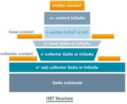
Construction: An HBT is a type of BJT (Bipolar Junction Transistor) that uses different semiconductor materials for the Base and Emitter regions. This creates a heterojunction. Figure 1 (above) illustrates the internal structure of an HBT.
-
Materials: HBTs are typically made using materials like InP (Indium Phosphide) or InGaAs (Indium Gallium Arsenide).
-
Performance: HBTs are capable of handling high-frequency signals, often in the range of several 100 GHz.
-
Applications:
- Fast switching RF circuits
- High power efficient devices, such as Power Amplifiers (PAs) used in mobile phones.
- Monolithic optical ICs (Integrated Circuits), such as PIN-based photo detectors.
HEMT - High Electron Mobility Transistor

-
Full Form: High Electron Mobility Transistor
-
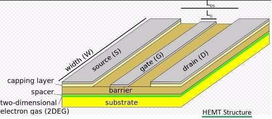
Construction: Figure 2 (above) shows the internal structure of a HEMT. It is a type of FET (Field-Effect Transistor) that incorporates a junction between materials with different band gaps (i.e., a heterojunction). Instead of using doped regions like in MOSFET designs, HEMTs use band gaps as channels.
-
Materials: HEMTs often utilize materials such as GaAs (Gallium Arsenide), AlGaAs (Aluminum Gallium Arsenide), and InGaAs.
-
Applications:
- HEMTs are typically used at very high frequencies, such as millimeter-wave bands.
- ON-OFF digital switches
- Low power amplifiers
- Satellite receivers
-
Advantages:
- Higher Gain
- Higher Switching Speed
- Low Noise
Difference Between HBT and HEMT
Following table mentions compatison between HBT and HEMT devices.
| Parameter | HBT | HEMT |
|---|---|---|
| Device Type | Bipolar Junction Device | Field Effect Transistor |
| Carrier Type | Both electrons and holes | Majority Carriers (Electrons only) |
| Control Mechanism | Current Controlled Device | Voltage Controlled Device |
| Junction Type | Heterojunction between emitter and base | Heterojunction forming 2D electron gas |
| Operating Principle | Current amplification via carrier injection | Channel conductivity controlled by gate voltage |
| Input Impedance | Low to Moderate | Very High |
| Switching Speed | Very High | Extremely High |
| Transit Frequency | High (100 to 500 GHz) | Very High (can exceed 500 GHz) |
| Noise performance | Moderate | Excellent (low noise) |
| Power handling | High | Moderate |
| Linearity | Excellent | Good |
| Power handling | High | Moderate |
| Typical materials | GaAs, SiGe, InP | GaAs, InP, GaN |
| Breakdown voltage | Lower | Higher, especially GaN HEMT |
Summary: This page provides a clear comparison between HBT and HEMT technologies, covering construction, carrier transport, gain and typical use cases. The explanation helps readers understand which transistor is more suitable for RF amplifiers, microwave ICs and high speed communication systems.
Advertisement
 RF
RF


