PLL Working: Understanding Phase Locked Loop Operation
Advertisement
This article explains the working operation of a Phase Locked Loop (PLL). It demonstrates the concepts using a PLL-based RF synthesizer application.
About PLL:
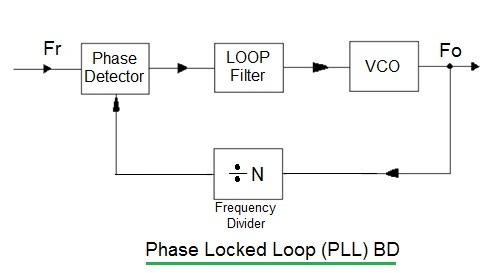
PLL stands for Phase Locked Loop. A basic PLL circuit consists of a Phase Detector, Loop Filter, Voltage Controlled Oscillator (VCO), and Frequency Divider.
PLL circuits are commonly found in RF frequency synthesizers or local oscillators within RF transceivers, which are used in RF frequency converters. Let’s dive into the operation of a Phase Locked Loop.

Figure 1: Block Diagram of a Phase Locked Loop (PLL)
Figure 1 shows the block diagram of a PLL circuit, which we’ll use to explain its working operation.
PLL Mathematical Equation
The fundamental equation governing a PLL is:
Fo = Fr * N
Where:
- Fo = Output Frequency
- Fr = Reference Frequency
- N = Division Ratio
Therefore, Fo can be altered to various values within a certain range by:
- Keeping Fr constant and changing N.
- Keeping N constant and changing Fr.
PLL Components and their Functions
Here’s a breakdown of the components used in a PLL:
-
Phase Detector (PD): Compares the reference frequency input with the output of the frequency divider. Based on this comparison, the PD generates an error voltage, which is then fed into the loop filter. In simple terms, a PD functions similarly to an EX-OR gate.
-
Loop Filter: Various configurations can be used for the loop filter. It’s essentially a low-pass filter that converts the error waveform output from the PD into a DC voltage used to tune the VCO.
-
Voltage Controlled Oscillator (VCO): The VCO changes its output frequency based on the applied DC error voltage. This allows it to adjust the frequency to compensate for any drift caused by temperature variations or aging. As a result, the frequency output of the PLL remains stable.
-
Frequency Divider (Divide by N): This component divides the PLL’s frequency output by an integer value (N). This ensures that the divided frequency is equal to, or close to, the input reference frequency used in the design.

As depicted in the block diagram above, an RF synthesizer comprises a phase comparator, frequency dividers, loop filter, VCO, PLL, and a reference clock oscillator.
The main idea behind this feedback and loop-based design is to lock the PLL’s frequency output to the reference frequency input, and to prevent any further drift caused by aging or temperature changes.
PLL Operating States
To understand the working principle of a PLL, let’s examine its three states:
-
Free Running State: Initially, when no reference frequency signal is applied, the PLL is said to be in a free-running state.
-
Capture State: When the reference signal frequency is applied, the VCO’s frequency begins to change. After a certain time, known as the frequency settling time, the PLL reaches a locked state. The state between the free-running and locked states is called the capture state. This represents the duration during which convergence occurs.
-
Phase Locked Loop State: This is the stable state where the loop has locked and the error voltage from the Phase Detector output is zero. This means the output frequency of the divider is equal to the reference frequency.
Applications of Phase Locked Loops
PLLs are used in a wide array of applications, including:
- Vector Signal Generators and Vector Signal Analyzers
- Function Generators
- Scalar Network Analyzers and Vector Network Analyzers
- RF Transceivers (RF Transmitters and RF Receivers)
- RF Local Oscillators and RF Synthesizers
Advertisement
 RF
RF


