 RF
RFVaractor Diode: Principles, Tuning Circuits, and Frequency Multipliers
Advertisement
A varactor diode is a semiconductor device that leverages the voltage-dependent capacitance of a semiconductor’s depletion region. It’s also known as a varicap diode or a tuning diode. These diodes are invaluable in electronic applications like tuning circuits, VCOs (Voltage Controlled Oscillators), frequency multiplier circuits, and frequency synthesizers. The varactor diode operates in reverse bias, relying on its transition capacitance.
In essence, the P and N regions of the diode have a high concentration of majority carriers, translating to low resistance. The space charge region (or depletion region), formed by the depletion of these majority carriers, acts as a dielectric. The P and N regions then serve as the plates of a capacitor. The depletion region acts as the insulating dielectric layer.
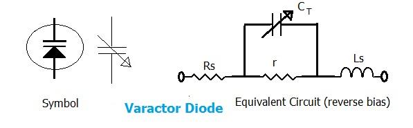
The reverse-biased P-N junction naturally exhibits junction capacitance due to the depletion region at the interface between the P-type and N-type materials. This is often called “transition capacitance” or “depletion capacitance”. It can be represented mathematically as:
Where:
- = Permittivity of the semiconductor
- = Area of the P-N junction
- = Width of the space charge region
Figure 1 (above) illustrates the varactor diode symbol and its equivalent circuit.
The transition capacitance, when considered in relation to the reverse bias voltage (), can be expressed as:
Where:
- = A constant dependent on the semiconductor material.
- = Diode knee voltage or barrier potential.
- = Reverse bias voltage.
- = 1/2 (for alloyed junction) or 1/3 (for diffused junction).
Varactor Diode Tuning Circuits
A varactor diode tuning circuit is a circuit that uses the voltage-dependent capacitance of a varactor diode to adjust the frequency or characteristics of another circuit such as an oscillator, filter or resonant circuit.
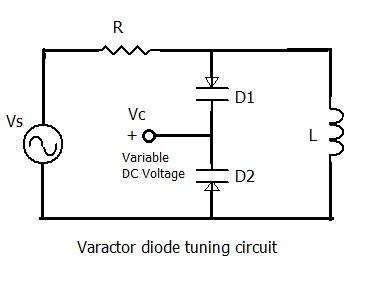
Figure 2 (above) depicts a typical varactor diode tuning circuit. In this example, two diodes, D1 and D2, provide a total variable capacitance within a parallel resonant circuit. represents the variable DC control voltage, which regulates the reverse bias and, consequently, the capacitance of the diodes. ‘L’ signifies the inductance in Henries. The resonant frequency of the tuning circuit is given by:
Where:
- (with and representing the maximum and minimum values of the diode capacitances, respectively).
Varactor Diode as a Frequency Multiplier
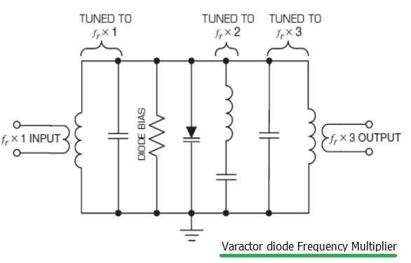
Diode frequency multipliers are commonly classified as either Schottky barrier diode or varactor diode types. Varactor diode multipliers utilize a nonlinear reactive element.
These reactive-type multipliers have the potential for high conversion efficiency. They require very low drive power levels but tend to have narrower bandwidths and exhibit a greater sensitivity to operating conditions. They can also present stability issues in some scenarios.
However, varactor diode frequency multipliers generate very little amplitude and phase noise. The primary noise source is the thermal noise from the series resistance of the varactor diode and any circuit loss resistances. The power handling capability of a varactor multiplier is limited by the breakdown voltage of the device. The varactor diode has a parasitic series resistance that dissipates power. A varactor frequency multiplier is capable of higher efficiency and higher power than a resistive type frequency multiplier.
Figure 3 (above) illustrates lumped element-based frequency doublers and triplers.
It is also possible to develop frequency doublers using microstrip elements along with varactor diodes. The varactor diode is connected in parallel with a capacitor in an LC tank oscillator. By changing the DC bias voltage on the varactor diode, its capacitance is altered, which in turn shifts the oscillator’s resonant frequency.
Advertisement


