 RF
RFSchottky Diode vs. P-N Diode: Key Differences Explained
Advertisement
This article compares Schottky diodes and p-n diodes, highlighting the fundamental differences between them. We’ll explore their symbols, structures, circuits, and characteristic curves.
P-N Diode
A p-n junction is the metallurgical boundary formed between the n-type and p-type regions within a semiconductor crystal. It consists of these two semiconductor regions with opposite doping types. These junctions exhibit significant rectifying behavior, leading to the creation of p-n diodes.
 Figure 1: P-N Diode Symbol
Figure 1 illustrates the standard symbol for a p-n diode.
 Figure 2: P-N Diode Structure
Figure 2 shows the structure of a typical p-n junction diode. As depicted, a p-n diode comprises a p-n junction with one connection to the p-side (anode) and another to the n-side (cathode).
 Figure 3: P-N Diode Characteristic
Figure 3 presents the characteristic curves for silicon and germanium diodes at 25°C. P-n diodes are commonly used as rectifiers in power supplies to convert AC to DC.
Silicon is generally preferred over germanium due to its superior properties:
- Much lower reverse current.
- Higher breakdown voltage.
- Ability to operate at higher temperatures.
Schottky Diode
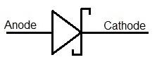 Figure 4: Schottky Diode Symbol
Figure 4 illustrates the symbol for a Schottky diode.
 Figure 5: Schottky Diode Structure and Circuit
In a Schottky diode, a metal-semiconductor junction is formed at one end, and another metal-semiconductor contact is made at the other. As shown in Figure 5, Schottky diodes use metals like tungsten, aluminum, chromium, platinum, or gold, and typically employ N-type silicon as the semiconductor material.
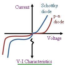 Figure 6: Schottky Diode Characteristic
Figure 6 shows the characteristic curve of a Schottky diode. The V-I curve is steeper compared to a standard p-n diode. Notably, Schottky diodes exhibit a lower forward voltage drop than p-n diodes.
Key Differences: Schottky Diode vs. P-N Diode
| Feature | Schottky Diode | P-N Diode |
|---|---|---|
| Forward Current | Occurs due to thermionic emission (majority carrier transport). | Occurs due to diffusion currents (minority carrier transport). |
| Reverse Current | Generated only due to majority carriers overcoming the barrier (less temperature-dependent). | Generated due to minority carriers diffusing to the depletion layer and drifting to the other side (more temperature-dependent). |
| Cut-in Voltage | Small (about 0.3V). | Large (about 0.7V). |
| Speed | High switching speed due to majority carrier transport; no recombination time needed. | Limited by the recombination time of injected minority carriers. |
| Ideality Factor | Approximately 1 due to no recombination in the depletion layer. | Approximately 1.2 to 2.0 due to recombination in the depletion layer. |
Advertisement


