 RF
RFSchottky Diode Basics: Construction, Characteristics, and Applications
Advertisement
This article covers the fundamentals of Schottky diodes, including their construction, advantages, and applications. The Schottky diode is a crucial microwave semiconductor device commonly used in various electronic circuits.
Figure 1 shows the circuit symbol for a Schottky diode.
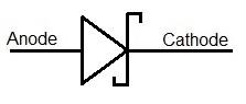 Schottky diode symbol
Schottky Diode Construction
The Schottky diode is built on a thin, heavily doped silicon (n+ type) substrate. An n-type active layer, approximately 2 microns thick, is grown epitaxially on this substrate. A thin layer of SiO2 (silicon dioxide) is then thermally grown over the active layer. Finally, a metal-semiconductor junction is formed by depositing metal over the SiO2 layer.
Schottky Diode Characteristics and Advantages
Schottky diodes possess several key characteristics that make them advantageous in specific applications:
- Square Law Characteristics: Schottky diodes exhibit a square law relationship between current and voltage, making them suitable for detector applications.
- High Burnout Ratings: They can withstand higher power levels compared to some other diode types.
- 1/f Noise: They exhibit 1/f noise characteristics (also known as flicker noise), which can be important to consider in sensitive applications.
- Better Reliability: Schottky diodes generally offer better reliability than point contact diodes.
These advantages make Schottky diodes a popular choice in various RF and microwave circuits.
Schottky Diode Applications
 Schottky diode and equivalent circuit
When a Schottky diode is forward biased, electrons (the majority carriers) are easily injected from the heavily doped n-semiconductor material into the metal. Conversely, when reverse biased, the barrier height increases, preventing electron flow and effectively blocking conduction.
These properties lead to several useful applications. RF power flow in the device is limited by power dissipation in Rs (series resistance). Rs is effectively shorted across Cj (junction capacitance), Cc (capacitance) and Ls (series inductance). These elements can cause RF mismatch, which can be addressed with an external matching circuit.
Advertisement


