MOSFET vs BJT: Key Differences Explained
Advertisement
This article explores the differences between MOSFETs (Metal-Oxide-Semiconductor Field-Effect Transistors) and BJTs (Bipolar Junction Transistors), two fundamental types of transistors used in electronics.
What is a MOSFET?
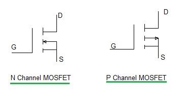
MOSFET stands for Metal Oxide Semiconductor FET.

MOSFET
There are two primary types of MOSFETs:
- n-channel MOSFET
- p-channel MOSFET
They can also be classified as:
- Depletion MOSFET
- Enhancement MOSFET
What is a BJT?
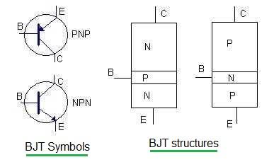
BJT stands for Bipolar Junction Transistor.

BJT
There are also two main types of BJTs:
- NPN transistor
- PNP transistor
For a clearer comparison, let’s examine the differences between an N-Channel MOSFET and an NPN type BJT.
MOSFET vs. BJT: A Detailed Comparison
Here’s a table summarizing the key differences between NPN BJTs and N-channel MOSFETs (NMOS):
| Feature | NPN BJT | N-channel MOSFET (NMOS) |
|---|---|---|
| Terminals | Three terminals: Base, Emitter, and Collector | Three terminals: Gate, Source, and Drain |
| Cutoff Region | { ; } | { ; } |
| Forward Active Region | { ; } | saturation(active) region { ; } |
| Reverse Active Region | { ; } | saturation(active) region { ; } |
| Saturation Region | { ; } | Triode region { ; } |
| Applied Voltage | ; between base and emitter junction | ; between Gate and Source terminals |
| Collector Current () | ||
| Base Charge (Q) | ||
| Base Transit Time () |
Understanding the Parameters
Here’s a breakdown of the parameters used in the equations above:
- : Applied voltage across Base and Emitter
- : Applied voltage across Gate and Source
- : Base-Emitter Junction Area
- : Width of Channel under gate
- : Length of channel under gate
- : Width of base region
- : Dopant density of p-type atoms in base
- : Gate Oxide capacitance per unit area
- : Threshold voltage
- (in NPN): Bulk mobility of electrons in the base
- (in NMOS): surface mobility of electrons in the channel
- : Diffusion constant of electrons in base
- : Intrinsic carrier concentration (strongly temperature dependent)
- : Electron charge
Advertisement
 RF
RF


