DMOS vs VMOS vs LDMOS: Understanding the Differences
Advertisement
This article compares DMOS, VMOS, and LDMOS transistors, highlighting the structural and functional differences between them.
DMOS Basics
DMOS stands for Double-Diffused MOS. These devices are frequently used in switching applications where high voltage and high frequency performance are crucial. You’ll also find them in applications like inkjet printheads, automotive control electronics, and power supplies.
DMOS Structure
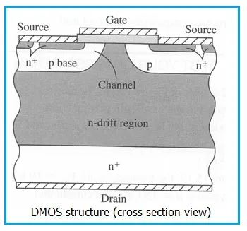
Figure 1 depicts a typical DMOS structure. Here are some key characteristics:
- Double Diffusion: DMOS devices are manufactured using a double diffusion process.
- Common Window: The p-region and the n+ source regions diffuse through a shared window, defined by the edge of the gate.
- Diffusion Depth: The p-region is diffused deeper than the n+ source region.
- Channel Length: The surface channel length is defined by the lateral diffusion distance between the p-substrate and the n+ source.
- Key Parameters: Breakdown voltage and on-resistance are critical performance metrics for DMOS devices.
- BJT Similarity: DMOS shares similarities with BJTs due to its high voltage and high-frequency capabilities.
- High Breakdown Voltage: Achieved through a lightly doped drift region between the drain and channel regions.
- N-Drift Region: A thinner n-drift region is desirable to minimize drain resistance.
VMOS Basics
VMOS stands for Vertical Metal Oxide Silicon. These devices feature a V-shaped gate region.
VMOS transistors are often used in medium-power applications such as power amplifiers and switching circuits.
VMOS Structure
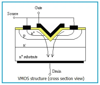
Figure 2 illustrates the VMOS structure. Key features include:
- V-Shaped Groove: The structure incorporates a distinctive V-shaped groove.
- Vertical Current Flow: The current flows vertically, from the source (at the top) to the drain (at the bottom), rather than horizontally.
- Larger Cross-Sectional Area: The V-shaped gate increases the cross-sectional area of the source-to-drain path. This results in a lower ON resistance, enabling higher power handling.
- Metallized Gate: The gate consists of a metallized area over the V-groove, controlling the current flow in the P-region.
- Complexity and Cost: VMOS structures are more complex than traditional FETs, making them more expensive to manufacture.
LDMOS Basics
LDMOS (Laterally Diffused MOS) is an asymmetric power MOSFET designed for applications requiring low on-resistance and high blocking voltage.
In LDMOS devices, the channel current is controlled by a vertical electric field (E) induced by the gate and a lateral field existing between the source (S) and drain (D).
LDMOS Structure
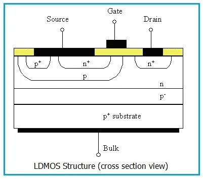
Figure 3 shows the LDMOS structure. Key aspects include:
- Channel Determination: The channel is defined by three parameters: gate length, drain diffusion, and source diffusion.
- Fabrication Process: LDMOS devices are fabricated using diffusion and ion implantation techniques.
- P-Type Region: Initially, a p-type region is constructed.
- Shallow Regions: Shallow p+ and n+ regions are then formed.
- Source and Drain Contacts: The source and drain contact regions are created from the n+ regions.
- Body Effect Elimination: The p+-region is connected to the p-type body and shorted to the source to eliminate the body effect.