 RF
RFDouble Heterojunction (DH) LED: Structure, Working, Advantages, and Disadvantages
Advertisement
This article explores the structure, operation, advantages, and disadvantages of the Double Heterojunction (DH) LED.
DH LED Structure and Working Operation
-
Structure: The figure below depicts a GaAs/AlGaAs based DH LED. A thin layer of GaAs is sandwiched between two layers of AlGaAs. The GaAs layer is lightly doped and has a narrower bandgap (Eg1) of about 1.43 eV. The AlGaAs layers have a wider bandgap (Eg2) of about 2.1 eV.
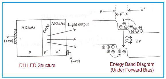
-
Working Operation:
- When a forward bias is applied through the top and bottom contacts, electrons are injected from the highly doped (n+) AlGaAs layer to the central active (p-) GaAs layer.
- The injected electrons are trapped within the middle layer due to the double heterojunction potential barriers (Eg2 > Eg1) existing on both sides of the middle layer. This creates a “quantum well” effect.
- The electrons are forced to recombine with holes without significant diffusion from the interfaces. They recombine radiatively with energy equal to the band gap of GaAs.
- Because recombination is limited to the narrower central part, the internal quantum efficiency of such an LED is higher compared to single junction LEDs.
- Moreover, GaAs and AlGaAs are lattice-matched, resulting in a very small surface density of defects.
- Emitted photons from the active region are not absorbed by the top and bottom AlGaAs layers due to the Eg2 > Eg1 condition (the AlGaAs is transparent to the light emitted by the GaAs).
- Due to these factors, the overall performance of the DH LED is improved.
Benefits (Advantages) of DH (Double Heterojunction) LED
- Offers higher efficiency with low to high radiance compared to single homojunction (p-n+) LEDs.
- Emitting wavelengths of GaAs/AlGaAs based DH LEDs range approximately between 0.8 to 0.9 µm. InP/InGaAsP based LEDs are used for longer wavelength radiation between 0.93 to 1.65 µm due to minimized signal attenuation in optical fibers at these wavelengths.
- Both the n-region and p-region are made out of wide bandgap materials (Eg > h*V), acting as optical windows and preventing absorption in these regions.
- The n-region and p-region can be highly doped.
- Injected electrons and holes are confined in a very narrow active region (i.e., a quantum well) where the n * p product is extremely high. Hence, the radiative recombination rate (R) is also high, leading to efficient light emission.
Drawbacks (Disadvantages) of DH (Double Heterojunction) LED
- These LEDs are most effective at low temperatures.
- The very small potential barrier encountered by electrons as they reach the p-side of the junction can limit performance.
- The growth process is complex and requires precise control over the materials and doping profiles.
Advertisement


