RF Wafer Probe Testing and On-Wafer Measurement Equipment
Advertisement
RF wafer probe testing, also known as on-wafer testing, is a crucial process in the characterization and testing of radio frequency (RF) and microwave devices on semiconductor wafers. This method allows for precise measurements of electrical parameters such as S-parameters, noise figure, and DC characteristics directly on the wafer. On-wafer measurement equipment is specialized for this purpose and includes several key components, as described below.
Let’s explore RF wafer probe testing, including on-wafer measurement and the equipment used for wafer tests.
On-Wafer Measurements
On-wafer measurements are a crucial aspect of semiconductor device testing, particularly in the field of radio frequency (RF) and microwave electronics. These measurements allow engineers to characterize the performance of semiconductor devices directly on the wafer, providing insights into their electrical properties, such as impedance, gain, noise figure, and linearity.
The on-wafer measurement process typically involves the following steps:
- Wafer Loading: The semiconductor wafer is loaded onto the prober station, and the alignment is adjusted to ensure proper positioning of the devices under test (DUTs) with respect to the RF probes.
- Probing: The RF probes make electrical contact with the DUTs on the wafer surface. Careful calibration and alignment are required to minimize contact resistance and parasitic effects.
- Measurement Setup: The measurement equipment, such as VNAs, spectrum analyzers, and noise figure analyzers, is connected to the RF probes. The measurement setup is configured to perform the desired measurements across the desired frequency range.
- Measurement Execution: The measurement software controls the equipment to perform the measurements according to the predefined test plan. RF and DC measurements are performed on each DUT on the wafer.
- Data Analysis: The measurement data is analyzed using specialized software to extract key parameters such as S-parameters, noise figure, gain, and phase. Statistical analysis may also be performed to assess device performance variability across the wafer.
- Reporting: The measurement results are compiled into a report summarizing the device characteristics, measurement conditions, and any anomalies or deviations from specifications.
The following table describes common on-wafer measurements:
| On-Wafer Measurements | Description |
|---|---|
| S Parameters | Various S parameters such as S11, S22, S12 and S21 are tested using VNA equipment. |
| Noise Figure | Lesser it is better is the DUT. It is essential for RF LNA test and measurements. Special equipments such as Noise Figure Meters are available for this test. |
| Pulsed Power | It is measured using RF Power Meter. Required for RF PA (Power Amplifier) testing. |
| Conversion Loss (e.g. IF to RF) | Required for RF Mixer. |
| Intermodulation products | Required for RF Amplifier, RF Transceiver. P1dB or TOI are the parameters required for this measurement. |
| Spectral measurements (e.g. ACPR, CCDF) | ACPR is the short form of Adjacent Channel Power Ratio and CCDF is the short form of Complementary Cumulative Distribution Function. |
| Modulation Accuracy measurements (EVM, BER or PER) | This used as modulation quality measurement as well as system performance under channel and other impairment environments. |
| RF Phase Noise | It is measure of purity of oscillator output or any signal generator output. Required to measure for RF LO, Signal Generator, RF Transmitter, RF Synthesizer etc. |
| Group Delay | It is required for vector device measurements. |
These measurements are essential for a wide range of applications, including wireless communications, radar systems, satellite communications, and more.
Wafer Test Equipment
On-wafer measurement equipment is specialized for this purpose and typically includes the following components.
-
Probe Stations: Probe stations are the primary test equipment used for on-wafer measurements. They consist of a precisely controlled stage where the semiconductor wafer is mounted, and probes are positioned to make electrical contact with the devices on the wafer. Probe stations offer features such as motorized movement for accurate positioning, temperature control for testing under different environmental conditions, and vacuum chucks for wafer stability.
-
Probes: On-wafer probes are specialized probes designed to make electrical contact with the devices on the wafer. These probes typically have very fine tips to ensure precise contact with the small features of semiconductor devices. They may be designed for RF/microwave applications to minimize signal loss and maintain high-frequency performance.
-
Vector Network Analyzers (VNAs): VNAs are essential for on-wafer RF and microwave measurements. They are capable of measuring S-parameters (e.g., , ) across a wide frequency range, providing detailed information about the device’s scattering parameters, impedance, and transmission characteristics. VNAs offer high accuracy and precision, making them indispensable for characterizing RF and microwave devices on-wafer.
-
Spectrum Analyzers: Spectrum analyzers are used for measuring the spectral content of RF signals. They are valuable for analyzing noise characteristics, spurious signals, and other RF phenomena. Spectrum analyzers can provide information about signal frequency, power, and noise figure, complementing the measurements obtained from VNAs.
-
Noise Figure Analyzers: Noise figure analyzers are specialized instruments used for measuring the noise figure of RF devices. They provide accurate measurements of noise characteristics, helping to assess the noise performance of amplifiers, mixers, and other RF components directly on the wafer.
-
DC Parameter Measurement Equipment: In addition to RF measurements, on-wafer testing often includes measurement of DC parameters such as current-voltage (IV) characteristics, capacitance, and resistance. Semiconductor parameter analyzers (SPAs) and other DC measurement equipment are used for this purpose.
-
Control and Analysis Software: Software plays a crucial role in on-wafer testing for controlling the measurement equipment, acquiring data, and analyzing results. The software allows engineers to automate test sequences, visualize measurement data, and extract key parameters from the measured data. It may also include advanced features for data analysis, such as statistical analysis and device modeling.
RF Wafer Probe Testing
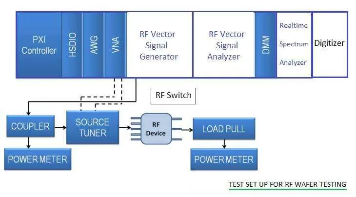
The figure-1 depicts RF Wafer test setup. As shown typical measurement setup covers equipments required to feed the signal input to the device under test(DUT) and equipments required to measure the output from the DUT. The signal generation equipments include vector signal generator, AWG etc. The signal analysis equipments include vector signal analyzer, digitizer, Oscilloscope, power meter, VNA etc.
On-wafer measurement equipment enables engineers to perform comprehensive characterization and validation of semiconductor devices directly on the wafer, providing valuable insights into device performance, optimizing device design, and ensuring product quality and reliability.
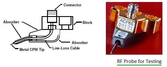
The microwave probe of various types such as air co-planar transition, ACP series probe and Infinity Series Probe are very popular in RF Wafer testing. They can easily be used to couple coaxial line to co-planar waveguide. They have small contact area and introduces very low contact resistance in the test setup. Figure-2 depicts one of the microwave probe of ACP type used for RF wafer testing.
On-Wafer Test Benefits
Following are the major benefits of RF wafer testing which has made it popular in RF and Microwave industry.
- The test setup calibration includes probe tip and hence the measurements are very accurate. This delivers high first pass design.
- Reproducibility of test results can be done with ease due to automatic alignment of modern test probes.
- Correlation between the wafer test results and module test results are excellent with minimum variation. Modules which use wafer devices should be properly grounded and should be DC biased as biased in the test setup.
- Production tests require very less cycle time.
- Higher throughput can be achieved in complete automated test setup. This also results into lower cost of testing.
Conclusion
RF wafer probe testing and on-wafer measurement equipment enable engineers to characterize the performance of RF and microwave devices with high accuracy and precision directly on the semiconductor wafer. These measurements are essential for optimizing device design, validating manufacturing processes, and ensuring the quality and reliability of RF components and integrated circuits.