Intel 8051 Microcontroller Architecture Explained
Advertisement
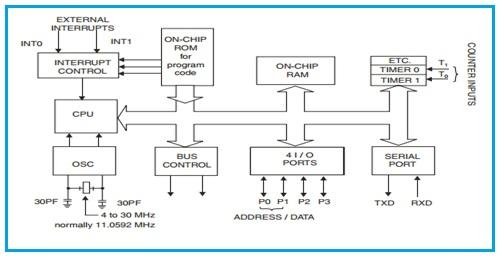
The Intel 8051 is a popular 8-bit microcontroller developed by Intel in 1980. It is widely used in various embedded systems and applications due to its versatility, simplicity, and ease of programming. The architecture of the 8051 microcontroller includes several key components, as described below.
The 8051 consists of the following internal elements or modules:
- 8-bit processor (CPU)
- Extensive Boolean processing (Single-bit logic) capabilities
- 64K Program Memory
- 64K Data Memory
- 4K bytes Program Memory (on chip)
- 128 bytes of Data RAM (on chip)
- 32 addressable I/O lines (bidirectional and can be individually addressed)
- Two 16-bit timer/counters
- Full-duplex UART
- 6-source OR 5-vector interrupts structure with two priority levels
- On-chip clock oscillator of 11.0592 MHz
Let’s understand these elements according to the 8051 architecture block diagram.
- CPU (Central Processing Unit): This 8-bit CPU is responsible for executing instructions. It has one accumulator and several general-purpose registers. It can be used for data manipulation and arithmetic instructions.
- Memory: The 8051 has two types of memory: program memory (ROM) and data memory (RAM). ROM stores the program code that the microcontroller executes, and RAM stores variables, intermediate calculations, and stack-related operations.
- I/O ports: It has four I/O ports (P0, P1, P2, P3). Port lines can be used to interface external devices. These port lines can be configured as input or output.
- Timers and counters: They are used to generate timing delays and to measure external events.
- Serial communications: It has a built-in UART (Universal Asynchronous Receiver Transmitter) for serial communication. It can be used for interfacing with other devices such as computers and other embedded devices.
- Interrupts: The 8051 supports both hardware and software interrupts. It has five interrupt sources and uses a prioritization scheme to handle interrupt requests.
- Clock circuitry: The Intel 8051 requires an external oscillator or clock source to provide the basic clock signal for its operation. The clock frequency and its variants determine the execution speed of instructions.
- Boolean processor: It is used to help in performing bitwise AND, OR, XOR, and complement operations on bits within registers.

The 8051 is a CISC-based architecture. The Intel 8051 follows the Harvard architecture principles of memory interface, so it has separate program and data memory. 16 of the available 32 I/O lines are used for accessing the external memory. We can access a maximum of 64KB of program and 64KB of data memory externally. 8 of the IO lines are used as both address and data lines. Both the program memory and data memories are 64K bytes. Program memory is read-only, and data memory is readable/writable. Program Store Enable is the read strobe signal used to access external program memory. There are RD and WR signals used for reading from and writing to the external memory. After a reset signal is applied to the microcontroller, program execution starts from the 0th location as stored in the program memory.
Microcontroller PSW (Program Status Word), BIT ADDRESSABLE

- RS0 and RS1: Selects the register bank to use.
- OV: Overflow Flag set by arithmetic operations.
- P: Parity bit set by hardware. If it contains an odd number of 1s, it is set, otherwise, it is zero.
- AC: Auxiliary Carry Flag (from addition operation).
- CY: Carry flag (from ALU operation).
Microcontroller PCON (Power Control Register), NOT BIT ADDRESSABLE

- PD: Activates power-down operation in microcontroller.
- IDL: Activates idle mode operation in microcontroller.
Conclusion
The 8051 microcontroller architecture has been widely used in various applications, including consumer electronics, automotive systems, industrial automation, and more.
Advertisement
 RF
RF


