HBM1 vs HBM2 vs HBM3: High Bandwidth Memory Comparison
Advertisement
This article breaks down the key differences between HBM1, HBM2, and HBM3 memory technologies. High Bandwidth Memory (HBM) is manufactured by companies like Samsung and Hynix and offers significant advantages over older memory types.
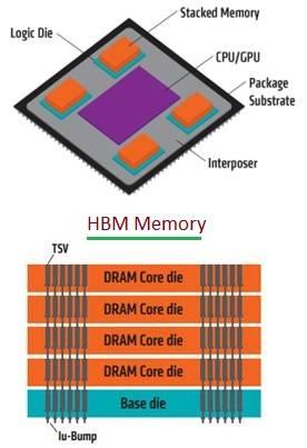
HBM is a non-planar memory solution, meaning it has a 3D structure, often described as a cube or cuboid. This allows memory chips to be stacked, resulting in a smaller footprint and enabling placement closer to the GPU.

Compared to GDDR memory, HBM provides lower power consumption, a smaller size, higher bandwidth, and overall improved performance.
HBM1 Memory
HBM memory, also known as stacked memory or compact memory, operates at around 1 Gbps. Its wide bus size enables significantly higher bandwidth compared to GDDR5. Specifically, it can achieve up to 128 GB/s of memory bandwidth per stack. HBM1 supports a capacity of 1GB per stack and 4GB per package, all while consuming less power than GDDR5 and GDDR5X.
HBM2 Memory
HBM2 represents the second generation of HBM, offering enhanced speed and bandwidth. Each stack incorporates 8 DRAM dies, with transfer rates reaching up to 2 Gbps. Thanks to its 1024-bit interface (twice that of HBM1), it delivers a bandwidth of 256 GB/s per stack. HBM2 also boasts a larger capacity than HBM1, offering approximately 8GB per stack. The Nvidia Tesla P100 card utilizes HBM2 memory, and it’s found in GPU architectures like Vega, Volta, and Pascal.
HBM3 Memory
HBM3 is the successor to HBM2 and brings even more improvements. It’s designed to be faster, consume less power, and support higher capacity compared to its predecessor. HBM3 can support up to 64 GB of VRAM in graphics cards and offers a memory bandwidth of up to 512 GB/s per stack.
Difference between HBM1, HBM2 and HBM3
The following table summarizes the key differences between HBM1, HBM2, and HBM3:
| Specifications | HBM1 | HBM2 | HBM3 (Expected) |
|---|---|---|---|
| Density per slice | 2 GB | 8 GB | 16 GB |
| Maximum speed | 1 Gbps | 2 Gbps | 3.2 Gbps |
| # of stack / Chip | 4 | 2/4/8 | 4/8/12/16 |
| Bandwidth/Chip | 128 GB/s | 256 GB/s | 410 GB/s |
| IO interface | CMOS | CMOS | Low voltage swing interface |
| Power consumption | Lower than GDDR5 and GDDR5X | Lower than HBM | |
| Manufacturers | Hynix, Samsung, Nvidia | Samsung, Hynix | |
| Appearance | Cube/ Cuboid | Cube/ Cuboid | |
| Graphics cards | Radeon R9, Fury X, Radeon Pro Duo | Nvidia Tesla P100, Nvidia Quadro GP100, Radeon Rx Vega 56, Radeon Rx Vega 64, Nvidia Titan V, AMD Radeon VII |
Advertisement
 RF
RF


