 RF
RFASIC vs FPGA: Design Flow and Implementation
Advertisement
ASIC (Application Specific Integrated Circuit) and FPGA (Field Programmable Gate Array) are both types of digital integrated circuits, but they differ in terms of their design, functionality, and use cases.
What is ASIC
Definition: ASICs are custom-designed integrated circuits built for a specific application or task. They are designed to perform a predefined set of functions and are optimized for efficiency and performance in that particular application.
Customization: ASICs are highly customized and tailored to a specific set of requirements. The design is often optimized for a particular algorithm or set of tasks, resulting in higher performance and lower power consumption.
Manufacturing: ASICs are manufactured using a specific process technology, such as CMOS (Complementary Metal-Oxide-Semiconductor). The design is finalized, and the circuit is fabricated as a unique chip for the intended application.
Advantages:
- High performance and efficiency.
- Lower power consumption.
- Cost-effective for high-volume production.
Disadvantages:
- High initial development costs.
- Longer development time.
- Not easily adaptable to changes or updates.
What is FPGA
Definition: FPGAs are programmable integrated circuits that can be configured and reconfigured by the user or designer after manufacturing. They consist of an array of programmable logic blocks and configurable interconnects.
Programmability: FPGAs provide flexibility as they can be programmed to implement a wide range of digital logic functions. This makes them suitable for prototyping, development, and applications with evolving requirements.
Customization: While not as optimized as ASICs, FPGAs offer a balance between customization and flexibility. They can be adapted for various applications by programming the logic elements.
Manufacturing: FPGAs are mass-produced, and users configure them based on their specific requirements. This allows for faster time-to-market and adaptability to changing needs.
Advantages:
- Flexibility and adaptability.
- Shorter development time.
- Suitable for low-to-medium volume production.
Disadvantages:
- Generally higher power consumption compared to ASICs for the same task.
- May have limitations in terms of performance for certain high-throughput applications.
ASIC and FPGA Design Flow and Implementation Steps
The design flow for ASICs (Application-Specific Integrated Circuits) and FPGAs (Field-Programmable Gate Arrays) involves several steps, each contributing to the overall process of designing, verifying, and manufacturing the digital integrated circuit. While there are similarities, there are also key differences in the design flow for ASICs and FPGAs. The most popular FPGA implementation is carried on Xilinx Virtex LX50 Evaluation board. ASIC synthesis is done on ST 65nm CMOS design kit.
ASIC Design Flow
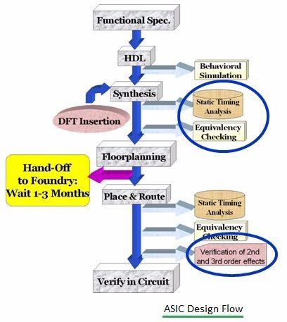
Figure-1 depicts ASIC design flow chart diagram and generic implementation steps are as follows.
- Specification: Define the functional requirements and specifications of the ASIC. This involves understanding the application, performance goals, and any specific features required.
- Architecture Design: Develop a high-level architectural design, defining the major functional blocks, data paths, and control structures of the ASIC.
- RTL Design: Create the Register-Transfer Level (RTL) description of the design using a hardware description language (HDL) like Verilog or VHDL. This step involves detailing the digital logic and the interconnections between registers.
- Functional Verification: Verify the correctness of the design through simulation and other verification techniques. Ensure that the RTL code behaves according to the specifications.
- Synthesis: Translate the RTL code into a netlist of logic gates. This involves synthesis tools that optimize the design for area, power, and timing.
- Physical Design: Place and route the synthesized netlist to create a physical layout. This step involves floor planning, placement of cells, and routing of interconnections.
- Timing Closure: Optimize the design for timing, ensuring that the clock frequencies and other timing requirements are met. Iterative changes may be made to achieve timing closure.
- Design for Testability (DFT): Integrate features into the design that facilitate testing, such as scan chains and built-in self-test (BIST) circuits.
- Functional and Timing Verification: Perform thorough verification to ensure that the physical design meets functional requirements and timing constraints.
- GDSII Generation: Generate the final GDSII (Graphic Data System II) file, which contains the detailed information needed for manufacturing the ASIC.
- Mask Manufacturing: Use the GDSII file to create photomasks for the semiconductor manufacturing process. This involves lithography and other processes to etch the circuit onto silicon.
- Wafer Fabrication: Manufacture the ASICs on silicon wafers through a series of semiconductor processes.
- Packaging and Testing: Package the fabricated ASICs and conduct thorough testing to identify and eliminate any defective chips.
FPGA Design Flow
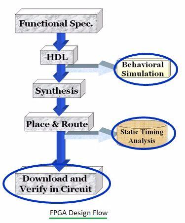
Figure-2 depicts FPGA design flow chart diagram and generic implementation steps are as follows.
- Specification: Define the functional requirements and specifications of the FPGA, considering the target application and desired performance.
- High-Level Design: Develop a high-level design, specifying the major functional blocks and their interconnections.
- RTL Design: Create the RTL description of the design using a hardware description language (HDL) like Verilog or VHDL.
- Functional Simulation: Simulate the RTL code to verify its correctness and functional behavior.
- Synthesis: Use synthesis tools to convert the RTL code into a netlist of configurable logic blocks (CLBs) and programmable interconnect.
- Place and Route: Place and route the synthesized design onto the FPGA architecture, considering the programmable resources and interconnects.
- Configuration Generation: Generate the bitstream or configuration file needed to program the FPGA. This file contains information about the placement and configuration of the logic elements.
- Programming: Program the FPGA with the generated bitstream or configuration file to implement the desired digital circuit.
- Functional Verification: Verify the functionality of the programmed FPGA through simulation or testing on the actual device.
- Integration and Testing: Integrate the FPGA into the target system and perform system-level testing to ensure it meets the overall requirements.
Difference between ASIC and FPGA
The following table mentions difference between ASIC and FPGA with respect to various features and comparison parameters.
| Feature | ASIC | FPGA |
|---|---|---|
| Full name | Application Specific Integrated Circuit | Field Programmable Gate Array |
| Customization | Highly customized and optimized for a specific application. | Programmable and offers flexibility, allowing for adaptation to different applications. |
| Development time | Longer development time, typically months to years | Shorter time to market, as FPGAs are already available and requires software porting work |
| Cost | Higher | Lower |
| Performance | Optimized for maximum performance in a specific application. | Good performance, but may not match the optimization level of ASICs. |
| Power consumption | Often more power-efficient due to optimization for specific tasks. | May consume more power due to programmable nature and additional overhead. |
| Volume and Scalability | Suitable for high-volume production. | Less scalable for small production runs or changing specifications. |
| More suitable for lower to medium production volumes, prototyping, and projects with changing specifications. | ||
| Reconfigurability | Fixed and cannot be reconfigured once manufactured. | Reprogrammable, allowing for quick updates and changes without physical redesign. |
| Applications | High-performance computing, networking equipment, specialized hardware. | Prototyping, telecommunications, image processing, embedded systems. |
| Example | ”Tensor Processing Unit” (TPU) developed by Google for machine learning tasks | ”Virtex UltraScale+” FPGA series from Xilinx |
Conclusion
From our comparison between ASIC vs FPGA we can conclude that, ASICs and FPGAs serve different purposes in the realm of digital ICs. ASICs are highly customized for a specific application, offering the best performance and efficiency for that task. FPGAs provide flexibility and can be adapted for multiple applications, but they may not achieve the same level of optimization.
Advertisement


