
FPGA Architecture and Basic Building Blocks
Advertisement
The architecture of an FPGA consists of logic blocks, a switch matrix, and I/O pads. The generic structure typically includes:
- Configurable Logic Blocks (CLBs)
- Input/Output Blocks (IOBs) or Pads
- Interconnection wires/switch matrix
Let’s explore these basic building blocks with a Xilinx example. The popular Xilinx Virtex-5 FPGA utilizes 6-input LUTs associated with multiplexers, logic, and flip-flops.
The key building blocks and features of the Virtex-5 FPGA are:
- Each CLB generally contains multiple slices, each with Look-Up Tables (LUTs) to implement combinational logic and flip-flops for storing sequential logic.
- Digital Clock Managers (DCMs) offer flexible clocking options.
- On-chip Block RAM can be used for data storage, FIFO buffers, and other memory-based functions.
- Some models include embedded PowerPC processor cores.
- High-speed RocketIO transceivers support serial communication protocols like Gigabit Ethernet, PCIe, and Serial RapidIO.
- SelectIO interface
- Embedded multiplier blocks
- External connectivity options for high-speed serial interfaces, external memory (DDR, DDR2, etc.), and general-purpose I/O pins.
- Supports various configuration modes, including JTAG.
Modern FPGAs can contain hundreds of thousands of CLBs. Sophisticated software like Xilinx ISE and ModelSIM are used for development and to generate the bitstream file for configuring the FPGA.
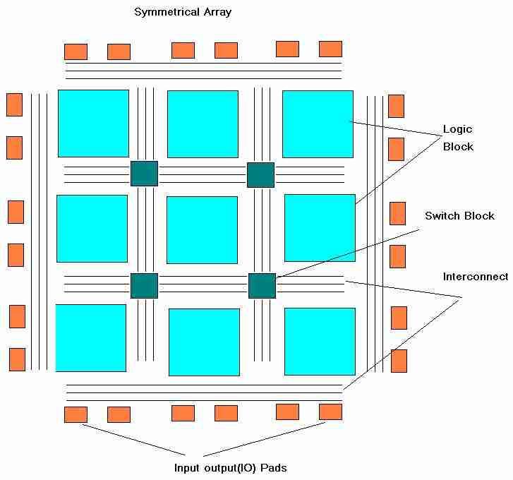
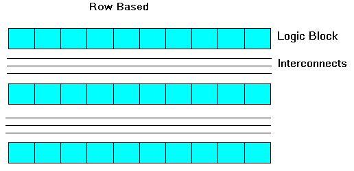
The Basic FPGA Architecture has 2-dimensional arrays of logic blocks with a configurable interconnection between the logic blocks and the function of each logic block.
The FPGA Architecture consists of the following building blocks:
1. Configurable Logic Blocks (CLBs)
- CLBs are fundamental building blocks responsible for implementing combinational and sequential logic.
- They typically include Look-Up Tables (LUTs), multiplexers, flip-flops, and other logic elements that can be configured to implement various logical functions.
Look-Up Tables (LUTs)
- LUTs are small memory units within CLBs that store pre-defined truth tables.
- They can be programmed to implement any Boolean logic function by configuring the input values and mapping them to the corresponding output values.
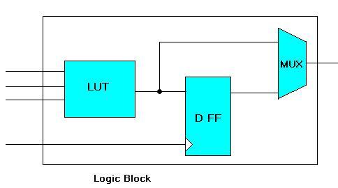
- Logic Block consists of LUT: It implements the combinational logic functions
- Register (e.g. D flip flip): it stores the output of LUT
- MUX: it is used for selection logic
- N-bit LUT is implemented as a 2n X 1 memory; Inputs choose one of 2n memory locations.
- Memory locations are loaded with values taken from configuration bit streams of the user.
- Inputs to Mux control are the CLB inputs.
Flip-Flops and Registers
- FPGAs contain a large number of flip-flops and registers that can be used to store and synchronize data within the design.
- These elements are crucial for implementing sequential logic and storing intermediate values during the operation of the circuit.
Clock Management
FPGAs often include dedicated clock management resources, such as PLLs (Phase-Locked Loops) and DLLs (Delay-Locked Loops), to generate and control clock signals within the design.
Block RAM (BRAM) and Distributed RAM
FPGAs include on-chip memory resources that can be configured as either block RAM or distributed RAM. Block RAMs are larger, dedicated memory blocks, while distributed RAM is spread across the CLBs.
Digital Signal Processing (DSP) Blocks
Many FPGAs include specialized DSP blocks optimized for arithmetic and logic operations, making them suitable for applications like signal processing.
Configuration Memory
FPGAs store their configuration information in non-volatile memory, typically SRAM-based or flash memory. The configuration memory contains the bitstream that defines the logic and interconnection of the FPGA.
2. Interconnection Resources
- FPGAs have a mesh of programmable interconnects that allow signals to be routed between different logic elements.
- These interconnects provide routing between the logic blocks to implement the user logic as per program.
- Switch matrices and programmable routing resources enable the configuration of connections between various CLBs and other components.
- Switch Matrix provides switching between interconnects depending on the logic.
3. Input/Output Blocks (IOBs)
- IOBs are responsible for interfacing with external devices and signals.
- These Input/Output pads are used for outside world to communicate in Applications.
- They include programmable input buffers, output buffers, and bidirectional buffers to adapt to different voltage levels and drive external signals.
4. Configuration Interface
FPGAs have a configuration interface that allows users to load the bitstream and configure the device. This interface can be parallel or serial, depending on the FPGA model.
Adaptive LUTs
The basic building block of an FPGA is the LUT (Look-Up Table) based function generator. The number of inputs to a LUT vary from three, four, six, and even eight after experiments. Now, we have adaptive LUTs which provide two outputs per single LUT with the implementation of two function generators.
Types of FPGAs based on Applications
Based on applications, FPGAs are categorized into three types: high-end FPGAs, low-end FPGAs, and mid-range FPGAs.
- High-end FPGAs: Developed for high performance and logic density.
- Low-end FPGAs: Developed for low complexity, low power consumption per chip, and low logic density.
- Mid-range FPGAs: Optical solution between the above two, developed as a balance between cost and performance.
Examples:
- High-end FPGAs: Virtex family from Xilinx, Stratix family from Altera, ProASIC3 family by Microsemi, Speedster 22i family from Achronix.
- Low-end FPGAs: Spartan family from Xilinx, Cyclone family from Altera, Mach XO/ICE40 from Lattice Semiconductor, Fusion family from Microsemi.
- Mid-range FPGAs: Artix-7/Kintex-7 series from Xilinx, Arria from Altera, ECP3 and ECP5 series from Lattice Semiconductor, and IGL002 from Microsemi.
Selecting an FPGA chip
The internal architecture elements mentioned above are crucial in selecting an FPGA chip based on the application.
Important selection parameters are:
- On-chip RAM size
- Input/output interfaces
- Device speed grade
- Number of DSPs or Multiplier blocks
- Operating temperature
- Package size
- Device density
- Input/Output pins
Besides the above parameters, the HDL code to be ported on the selected FPGA chip will decide whether the selected device is sufficient to store the logic for the application under development. The same can be inferred from the synthesis cycle count report.
Due to the availability of advanced high-end FPGAs, they have become an alternative to ASIC and ASSP. Some vendors are marketing FPGAs suitable for testing the code before ASIC implementation.
ARM-based System On Chips (SoCs) combine processors, memory controllers, and peripherals with custom FPGA in a single chip. Now FPGAs are available in 45nm, 28nm, 20nm, and 16nm. Research is ongoing to develop 14 and 10nm devices soon.
Conclusion
Understanding the FPGA architecture and basic building blocks is essential for effectively designing and implementing custom digital circuits using these versatile devices.
Users program FPGAs using Hardware Description Languages (HDLs) like Verilog or VHDL. The design is then synthesized and mapped to the architecture of the FPGA using specialized tools provided by FPGA vendors such as Xilinx.
Advertisement


