 RF
RFNoise Generation Sources & Reduction Techniques
Advertisement
Noise in electronic systems can significantly affect performance and reliability. This article explores various noise reduction techniques, from shielding to active noise cancellation, offering practical solutions to minimize unwanted disturbances.
Introduction
As we know, noise or interference cannot be completely eliminated but can be reduced or minimized. A system is electromagnetically compatible if it satisfies the following three criteria:
- It does not cause interference to other nearby systems.
- It is not susceptible to emissions or radiations from other systems.
- It does not cause interference to itself.
Interference occurs when a receiver or receptor receives energy which causes it to behave in an undesired manner. There are two main types of interference: direct and indirect. Examples of direct interference are common impedance coupling through the conductor, etc. Examples of indirect interference are crosstalk, radiation, etc.
Figure 1 depicts these sources of noise or interference.
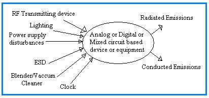
Noise Generation Sources
There are two major terminologies: EMI and EMC. The sources of EMI include the following:
- Common sources of electromagnetic emissions are lighting, motors, lights, relays, etc.
- Cables, AC power conductors, metal cabinets, and other circuits receive or radiate undesired signals.
- Clock circuits used in digital circuits generate wideband noise. Other elements are RESET lines, CONTROL, and INTERRUPT lines.
- Open wires such as power supply leads pick up noise into the circuit. This is an example of conductive EMI.
- When two circuits are connected with a common impedance path, a noise signal is coupled from one circuit to the other and vice versa due to the flow of ground currents.
- When there are two nearby conductors, the flow of current in one conductor causes radiation to the other conductor and vice versa. This is known as crosstalk.
- Die size, pad layout, and packaging can also affect EMI.
- Improper PCB layout for different sections of the circuit (e.g., analog, digital, high frequency) can also cause EMI.
- Power supply lines should be properly connected to the circuit.
The sources of EMC include the following:
- High supply voltages will have greater voltage swings and hence will have more emissions.
- High frequency values as well as periodic signals cause more emissions.
- Noise is created due to current spikes. In digital systems, current spikes are created during switching ON/OFF of the transistors. The load current variation causes current spikes in analog systems.
- Improper grounding is another source of noise. There are different types of grounding for different types of circuits: single point grounding (below 1 MHz), multipoint grounding (high frequency digital circuits), and hybrid grounding. Hybrid types use both single point for low frequency and multipoint for high frequency. The proper ground and power plane layout should be made for PCBs after segregating digital, analog, and high frequency noisy parts.
The following are the major techniques to reduce the noise in the device or PCB. These techniques will help in improving the performance of noisy systems. There are many more ways to improve the performance based on various applications or products.
- Try to suppress emission at its source itself.
- Make the coupling path most inefficient.
- Make the receiver less susceptible to radiation or emission.
Noise Reduction Techniques at Device Level
The following noise reduction techniques are commonly used at the device level:
- Use multiple power pins and ground pins.
- Use as few clocks as possible.
- Try to reduce output buffer drive.
- Eliminate race conditions.
- Keep more space between low-speed traces and high-speed traces. Run high frequency signal traces next to the ground bus.
- Keep clock lines off when they are not in use.
- Eliminate charge pumps if possible to do so.
- Keep the loop area as small as possible inside the chip.
- Make use of low power methods.
- Reduce internal impedance of the power trace and ground trace.
- Provide good ground imaging for long traces as well as traces carrying high-speed signals.
Noise Reduction Techniques at Board Level
The following noise reduction techniques are commonly used at the PCB or board level:
- Make use of ground planes and power planes on the board.
- Minimize the use of surface conductors on the PCB.
- Maximize plane areas in order to provide lower impedance for decoupling of the power supply.
- Make use of narrow traces (about 4 to 8 mils) to increase high-frequency damping and to reduce capacitive coupling.
- Segregate circuits on the PCB based on frequency (e.g., low/high) and type (e.g., analog/digital).
- Segment GND/Power for analog, digital, transmitter, receiver, etc.
- Do not notch or cut the PCB. This often creates unwanted loops due to nearby traces.
- Avoid large open loop structures during PCB design.
- Design multi-layer boards so that traces between the power plane and ground plane are enclosed properly.
- Use chassis ground. This shielding helps to prevent radiation at circuit boundaries.
- Use proper grounding types such as single point for low frequency and multipoint for high frequency portions on the PCB.
- Keep ground leads shorter than (1/20)th of λ in order to prevent radiation and to maintain lower impedance.
- Do proper routing of traces e.g., use 45 degrees instead of 90 degrees for trace turns, route clock signals perpendicular to I/O lines, etc.
- Use appropriate filters at different places on the PCB. Filter the power line and all signals entering into the PCB. Use appropriate decoupling capacitors at power pins. Use ferrite beads at power entry inputs. Use bypass capacitors at appropriate places on the PCB. Make use of multistage filters to attenuate multiband power supply noise.
Conclusion
Implementing effective noise reduction techniques can improve signal integrity and overall system performance. Understanding these methods ensures robust and reliable electronic designs.
Advertisement


