The Versatile 555 Timer IC
Advertisement
The 555 timer IC is a remarkably adaptable chip, a true workhorse in electronics. Introduced in 1972 by Signetics (now part of ON Semiconductor), it has become a staple in countless applications, particularly in the realm of digital pulse generation.
This IC’s versatility shines through its ability to be configured in three primary modes: Monostable, Astable (free-running), and Bistable (Schmitt Trigger). Let’s delve into the pin diagram and internal workings of this ubiquitous component.
Internal Circuitry
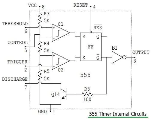
As illustrated above, the 555 timer comprises several key elements: two operational amplifiers acting as comparators (C1 and C2), an RS bistable element (FF), an inverting output buffer (B1), and a transistor switch (Q14). The inverting buffer is crucial, enabling the IC to source or sink a considerable amount of current to/from a load. The transistor switch (Q14) provides a means to rapidly discharge the external timing capacitor.
Pin Diagram and Descriptions
The standard 555 timer comes in an 8-pin DIP (dual in-line package). Several variations exist, including the NE555, LM555, and TLC555, each with slight differences in specifications and performance.
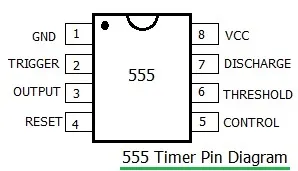
The following table describes each pin of the 555 IC:
| Pin Number | Description |
|---|---|
| 1 | GND (Ground Connection) |
| 2 | Trigger (Triggers when this pin transitions from Vcc to 33% of Vcc. Output goes high when triggered) |
| 3 | Output (This pin delivers the output signal) |
| 4 | Reset (Resets the 555 timer when pulled low) |
| 5 | Control Voltage (Used to change ‘threshold’ and ‘trigger’ set point voltages; rarely used) |
| 6 | Threshold (Detects when the capacitor has charged to 66.6% of Vcc, causing the output to go low) |
| 7 | Discharge (Used to discharge the capacitor) |
| 8 | +VCC (Supply voltage input, typically 5V to 15V) |
Astable Mode
The Astable mode configures the 555 timer as a free-running oscillator.
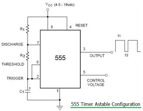
In this configuration, the trigger pin is connected to the capacitor, and a resistor is placed between the discharge and threshold pins. Unlike the Monostable mode, the Astable circuit triggers from the previous output pulse, eliminating the need for an external trigger. The output pin continuously oscillates between high and low, generating a series of pulses as the capacitor charges and discharges between 33.3% and 66.6% of Vcc.
The duration the output pin stays high () is:
The duration the output pin stays low () is:
The frequency () of the output pulses is:
Applications of the 555 Timer in Astable Mode:
- Modulation of ultrasonic and IR transmitters.
- Turning an actuator ON and OFF at set intervals for a fixed duration.
- Generating accurate clock signals.
Monostable Mode
In Monostable mode, the 555 timer acts as a “one-shot” pulse generator.
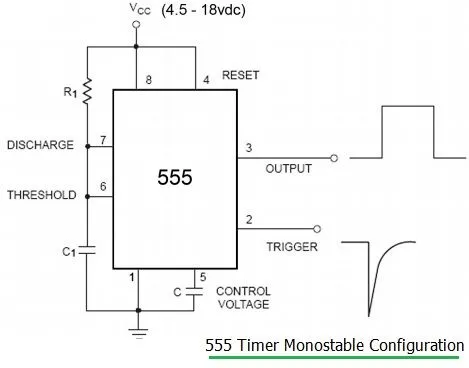
The Monostable circuit produces a single output pulse for each high-to-low transition on the trigger pin. The output returns to its “stable” state after a period determined by the resistor and capacitor values. The output pulse length is determined by the time it takes the capacitor to charge to 66.6% of Vcc, a rate governed by the capacitor’s capacitance (C1) and the resistor’s resistance (R1).
The length of the output pulse () is:
Applications of the 555 Timer in Monostable Mode:
- Debouncing momentary or push-button switches.
- Turning on an actuator for a set duration.
- Converting an analog signal from a resistive sensor into a digital signal.
Conclusion
The 555 timer IC remains popular for its ease of use, affordability, and widespread availability. It’s an excellent starting point for those learning electronics and a valuable tool for engineers designing various timing and control circuits. From LED flashers and pulse generators to timers, oscillators, and PWM (pulse-width modulation) generators, the 555 timer continues to prove its worth in a multitude of applications.