 RF
RF8085 Microprocessor Architecture: Pinout and Block Diagrams Explained
Advertisement
The Intel 8085 is an 8-bit microprocessor introduced by Intel in 1976. Key features of the 8085 chip include an 8-bit data bus, a 16-bit address bus, a 3.072 MHz internal clock frequency, and a 40-pin configuration. It operates using a +5V supply voltage.
The internal architecture of the 8085 microprocessor can be understood through two primary diagrams: the block diagram and the pin diagram.
8085 Microprocessor Architecture
The 8085 chip is an 8-bit general-purpose microprocessor capable of addressing 64KB of memory.
The 8085 architecture comprises registers, flags, and counters.
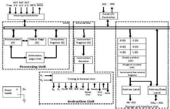
Figure - 1: Block diagram of the 8085 microprocessor
Figure 1 illustrates the internal architecture of the 8085 microprocessor. Broadly, the 8085 architecture consists of three units:
-
Processing Unit
-
Instruction Unit
-
Storage and Interface Unit
-
Processing Unit: Consists of the Arithmetic Logic Unit (ALU), Accumulator, Status Flags, and a Temporary Register.
-
Instruction Unit: Comprises the Instruction Register, Instruction Decoder, and Timing and Control Unit.
-
Storage and Interface Unit: Includes general-purpose registers, Stack Pointer (SP), Program Counter (PC), Increment/Decrement Register, Address Latch, and Address/Data Latch.
The architecture also includes an Interrupt Controller, Serial I/O Controller, and Power Supply unit, as shown in the figure. All these hardware modules and their respective pins are depicted in the diagram.
8085 Pin Diagram
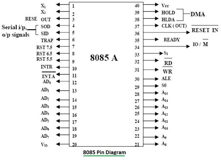
Figure 2: Pin Diagram of the 8085 Microprocessor
Figure 2 illustrates the 8085 pin diagram. The 8085 microprocessor has 40 pins, operates with a +5V supply, and runs at a maximum frequency of approximately 3 MHz.
The pins on the 8085 chip can be grouped into six categories:
- Address Bus
- Data Bus
- Control and Status Signals
- Power supply and frequency
- Externally Initiated Signals
- Serial I/O ports
8085 Pin Description
| Pin | Description |
|---|---|
| AD0 to AD7 | These are bi-directional pins serving as both the address and data bus. During instruction execution, these lines initially act as the address bus and later as data bus lines. An external latch is interfaced with these lines. |
| A8 to A15 | These are unidirectional address bus lines. |
| ALE | (Address Latch Enable) - A pulse that holds a value of 1 when AD0-AD7 lines are used as the address bus and then becomes 0. This signal is used to enable the externally connected latch. |
| RD’ | Read signal (active low). |
| WR’ | Write signal (active low). |
| IO/M’ | This signal specifies whether the operation is a memory operation (IO/M’ = 0) or an I/O operation (IO/M’ = 1). |
| S1, S0 | These are status signals indicating the type of operation being performed by the 8085 microprocessor. |
Status Signals:
| S1 | S0 | Function |
|---|---|---|
| 0 | 0 | HALT |
| 0 | 1 | WRITE |
| 1 | 0 | READ |
| 1 | 1 | FETCH |
| Pin | Description |
|---|---|
| SID | Serial Input Data line. The data on this line is loaded into accumulator bit-7 whenever a RIM (Read Interrupt Mask) instruction is executed. |
| SOD | Serial Output Data line. The output SOD is set or reset as specified by the SIM (Set Interrupt Mask) instruction. |
| INTR | Input, Interrupt Request. It is used as a general-purpose interrupt. INTR is enabled and disabled by software. It is disabled by reset and immediately after an interrupt is accepted. |
| INTA’ | Output, Interrupt Acknowledge. This signal is used instead of RD’ during the instruction cycle after an INTR is accepted. It can be used to activate an 8259 interrupt chip or other interrupt port. |
| RST5.5, RST6.5, RST7.5 | These are three interrupt inputs that have the same timing as INTR, except they automatically insert an internal RESTART. RST 7.5 has the highest priority, and RST 5.5 has the lowest. These interrupts have higher priority than INTR. |
| TRAP | Input, TRAP interrupt is a non-maskable restart interrupt, unaffected by any mask or interrupt enable. It has the highest priority of any interrupt. |
| RESET IN | (Input) Reset sets the Program Counter (PC) to zero, resets interrupt enable and HLDA flip-flops. None of the other flags or registers are affected. The CPU is held in reset as long as RESET is applied. |
| RESET OUT | (Output) Indicates the CPU is being reset. It can be used as a system RESET. The signal is synchronized to the processor clock. |
| CLK OUT | An output clock pin to drive the clock of the rest of the system. |
| READY | (Input) If this signal is high during a read or write cycle, it indicates that memory or the peripheral is ready to send or receive data. If READY is low, the CPU will wait for READY to go HIGH before completing the read or write cycle. |
| HOLD | (Input) HOLD indicates that another MASTER is requesting the use of the Address and Data Buses. Upon receiving the Hold request, the microprocessor (CPU) will relinquish the buses upon completion of the current machine cycle. Internal processing can continue. The processor can regain the buses only after the Hold is removed. |
| HLDA | (Output) HOLD ACKNOWLEDGE - Indicates that the CPU has received the Hold request and will relinquish the buses in the next clock cycle. HLDA goes low after the Hold request is removed. The CPU takes the buses one half clock cycle after HLDA goes low. |
| VCC | +5V supply |
| VSS | Ground Reference |
| X1, X2 | These signals are inputs from a crystal or clock generator. |
Conclusion
The Intel 8085 microprocessor is a classic and widely used microprocessor in computer engineering education for teaching basic concepts. Over the years, numerous other significant microprocessor architectures have been developed. The latest microprocessors include Intel 8086/8088, Motorola 68000 series, Intel 80286, Intel 80386, Intel Pentium, and other modern architectures such as ARM, RISC-V, and so on.
Advertisement


